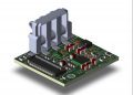
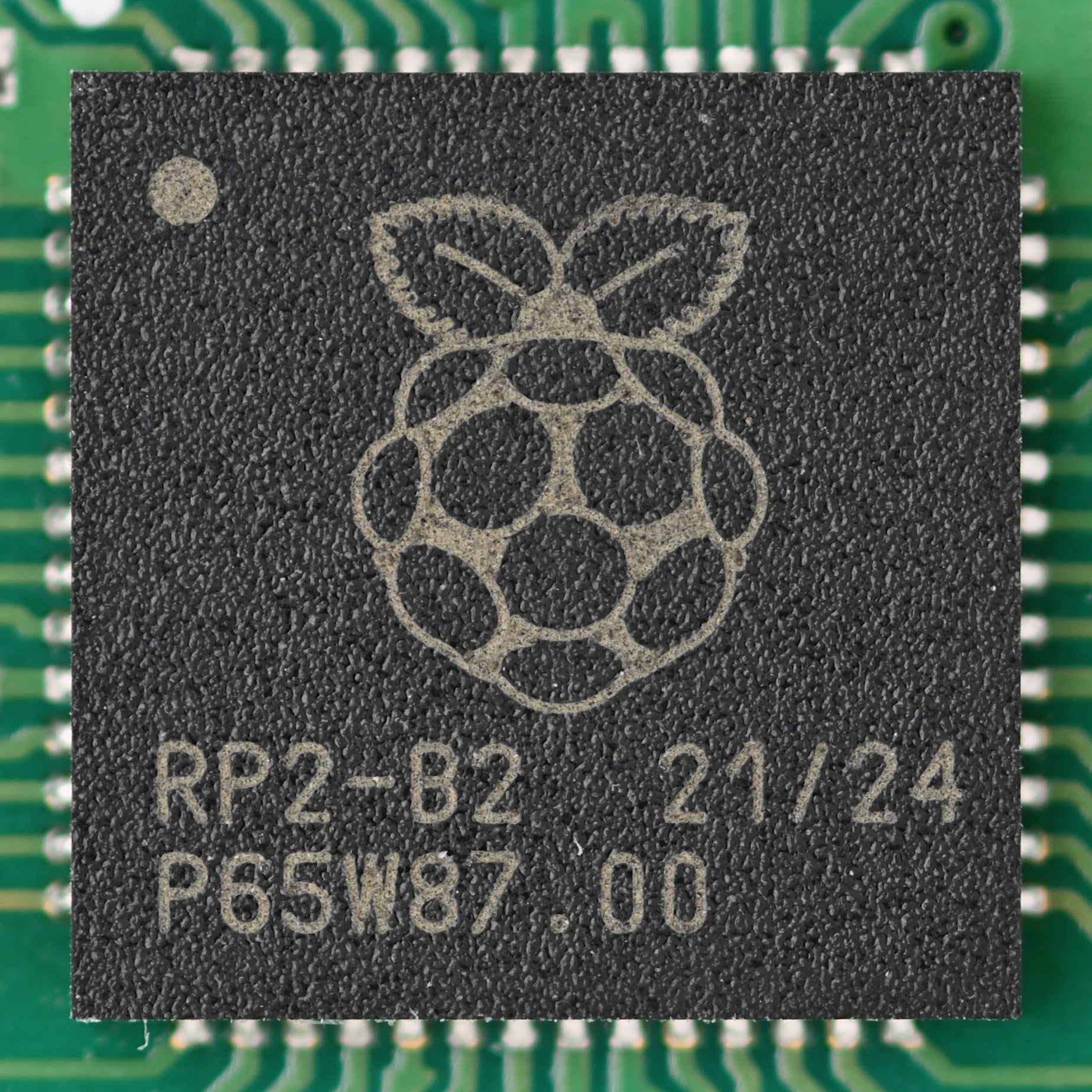
RP2040 microcontroller, the driver of the multifunction RP2040 Zero development board.
The RP2040 Zero packages Raspberry Pi’s dual-core RP2040 microcontroller into a 23.5 mm × 18 mm footprint that works as a standalone development board or a surface-mount daughterboard on a custom PCB. Rather than building power management, clock circuitry, and external flash from scratch, engineers can drop it straight into their design. Understanding the RP2040 Zero datasheet is key to keeping power design, pin usage, and electrical limits on the reliable side.
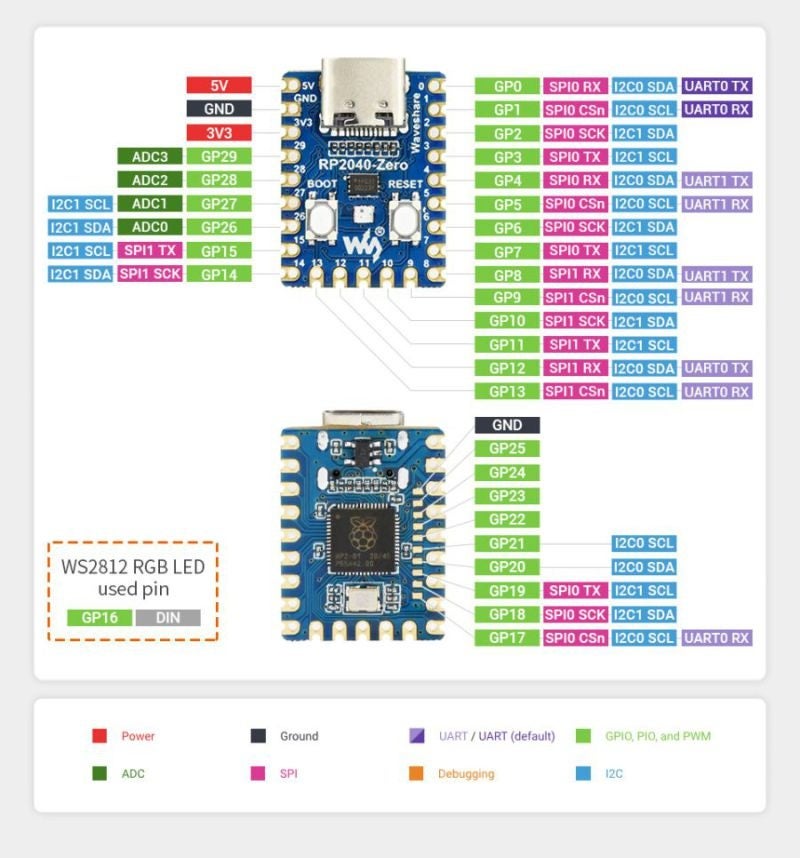
RP2040 Zero Pinout and Internal Architecture
Pin
RP2040 Function
Description
5V (VBUS)
USB Power Input
5V power supplied from the USB-C connector or an external 5V source. Used as the input to the onboard voltage regulator.
3V3
Regulated Power Output
Regulated 3.3 V output from the onboard LDO regulator (total rated capacity: 500 mA). After internal consumption by the MCU, flash, and WS2812 LED, approximately 300 mA remains available for external circuits, depending on system load.
GND
Ground
Common ground reference for the board. Internally connected to the RP2040 ground pads.
GPIO0–GPIO15
GPIOx
General-purpose digital I/O pins supporting peripheral functions including Universal Asynchronous Receiver-Transmitter (UART0/UART1), Inter-Integrated Circuit (I2C0/I2C1), Serial Peripheral Interface (SPI0), Pulse Width Modulation (PWM) channels 0–3, and Programmable I/O (PIO) state machines.
GPIO16
GPIOx
Connected internally to the onboard WS2812 RGB LED. Not exposed on the header for general use.
GPIO17–GPIO25
GPIOx
Additional general-purpose digital I/O pins accessible only through underside solder pads. Support the same peripheral functions as other GPIOs.
GPIO26–GPIO29
GPIOx / ADCy
General-purpose digital I/O with integrated 12-bit ADC capability (ADC0–ADC3) for measuring analog voltages. These pins are located on the perimeter castellated headers and are accessible without soldering to the underside pads.
QSPI0–QSPI5
QSPIx
Dedicated Quad-SPI interface used to connect the onboard external flash memory with execute-in-place (XIP) support. These pins can also function as GPIO if flash access is not required.
USB_DM / USB_DP
USB Interface
Dedicated Full-Speed USB data lines supporting USB device mode and Full-/Low-Speed host mode. Internal pull-up and pull-down resistors are provided.
XIN / XOUT
Crystal Oscillator
Connects the external 12 MHz crystal oscillator or an external clock source used by the RP2040 system clock.
RUN
Reset Input
Active-low asynchronous reset pin. Pulling RUN low resets the RP2040.
SWCLK / SWDIO
Serial Wire Debug (SWD)
Debug and programming interface providing access for firmware upload and debugging.
TESTEN
Factory Test
Factory test pin. Tie to GND during normal operation.
IOVDD
GPIO Power Supply
Supply voltage for the RP2040 digital GPIO bank (1.8–3.3 V). On the RP2040 Zero, this is normally connected to the regulated 3.3 V rail.
The RP2040 Zero features a dual-core ARM Cortex-M0+ processor running at up to 133 MHz. Memory includes 264KB of embedded SRAM distributed across six independent banks, allowing parallel access by both processing cores and the direct memory access (DMA) controller. Program code resides on an onboard 2MB Quad-SPI Flash chip connected via an eXecute In Place (XIP) bus.
To support complex peripheral interfaces without straining CPU resources, the internal architecture integrates eight Programmable I/O (PIO) state machines. These state machines execute simple, deterministic assembly programs that emulate custom hardware protocols, such as I2S audio, VGA video, or specialized LED drivers, independently of the main CPU cores.
Of the 30 GPIOs supported by the RP2040 silicon, the RP2040 Zero routes 29 to physical access points. 20 pins line the perimeter on two 10-pin, 2.54 mm pitch headers, while 9 additional GPIOs are accessible via solder pads on the underside of the PCB.
Pinout of RP2040 Zero development board.
RP2040 Zero Datasheet Key Specifications
The specifications below define the electrical and operational boundaries for the RP2040 Zero. Push past them, and you risk unpredictable behavior or permanent damage to the chip. Keep these as firm limits when you’re building out your schematic and laying out the board.
Electrical Characteristics and Operating Limits
Parameter
Specification
Notes
Input Supply Voltage (VBUS)
4.0 V to 5.5 V DC
Powered via USB-C or Pin 1
Logic Level Voltage
3.3 V I/O
Not 5V tolerant; exceeding 3.3 V damages GPIOs
Max Onboard LDO Output
500 mA
Shared between MCU, flash, LED, and external loads
Max Output Drive (Per GPIO)
12 mA
Software configurable (2 mA, 4 mA, 8 mA, 12 mA)
Max Total GPIO Bank Current
50 mA
Cumulative limit across all active digital I/O pins
Onboard Flash Memory
2MB (16 Mbit)
Quad-SPI W25Q16JV or equivalent
Active Current Draw
18 mA to 50 mA
Varies with clock frequency and active peripherals
Sleep Mode Current
~1.3 mA
System clocks running, ARM cores halted
Dormant Mode Current
~180 µA
All internal clocks and PLLs disabled
Notably, the RP2040 Zero datasheet specifies that all GPIO pins operate strictly at a 3.3 V logic level. Connecting 5V signals directly to any GPIO pin will damage or destroy the input buffer. If you’re connecting 5V sensors or older logic systems, use bidirectional logic level shifters or resistor voltage dividers.
The onboard ME6211 low-dropout (LDO) linear regulator converts the 5V supply to a stable 3.3 V rail. While the regulator can deliver up to 500 mA, the internal RP2040 MCU, flash memory, and WS2812 LED consume a portion of this budget. When powering external sensors or expansion modules from Pin 3 (3V3), keep external current draw below 300 mA to avoid heat buildup or voltage drop on the regulator rail.
Furthermore, cumulative current limits across the GPIO bank require careful management. While an individual pin can source up to 12 mA in high-drive mode, drawing maximum current from multiple pins simultaneously will exceed the 50 mA total bank limit. For driving high-current loads such as relays, solenoids, or high-brightness LEDs, route GPIO signals through discrete MOSFETs or dedicated gate drivers.
RP2040 Zero vs. Alternative Development Boards
Selecting the right development module requires evaluating physical dimensions, exposed pin counts, and onboard feature sets against project requirements.
RP2040 Reference Boards Comparison
Board Name
Dimensions
Exposed GPIOs
Onboard Flash
USB Connector
Onboard RGB LED
Primary Use Case
Waveshare RP2040 Zero
23.5 mm × 18.0 mm
29
2MB
USB Type-C
Yes (WS2812)
Space-constrained carrier PCBs
Raspberry Pi Pico
51.0 mm × 21.0 mm
26
2MB
USB Micro-B
No
Standard breadboard prototyping
Adafruit QT Py RP2040
21.8 mm × 17.8 mm
11
8MB
USB Type-C
Yes (NeoPixel)
Qwiic/STEMMA QT sensor nodes
SparkFun Pro Micro RP2040
33.0 mm × 17.8 mm
20
16MB
USB Type-C
Yes (WS2812)
Compact commercial products
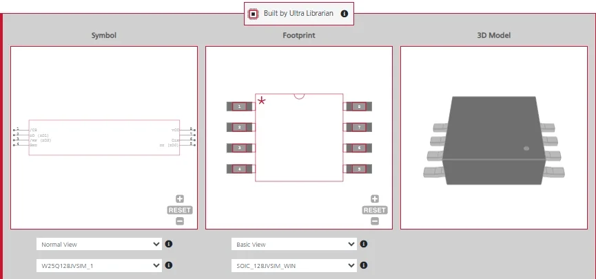
All four boards listed above have verified CAD models available through Ultra Librarian, so you can pull footprints, schematic symbols, and 3D STEP files for any of them without building from scratch. While the official Raspberry Pi Pico provides a larger canvas with standard mounting holes, its 51 mm length makes it unsuitable for ultra-compact enclosures. The RP2040 Zero cuts physical board area by more than 60% while exposing three additional GPIO pins compared to the Pico.
When compared to the Adafruit QT Py RP2040, the RP2040 Zero offers significantly more raw I/O pins (29 vs 11), making it better suited for designs requiring extensive parallel connections, matrix keypads, or multiple SPI/I2C buses. The SparkFun Pro Micro RP2040 is a solid middle-ground option, trading some I/O (20 GPIOs) for a larger 16 MB flash footprint. It’s worth considering for commercial products where additional onboard storage matters more than maximum pin count.
Hardware Integration and Troubleshooting Guidelines
After assembling the board or recovering firmware, run a simple test program to verify basic functionality before integrating application code.
Onboard WS2812 RGB LED Test: Cycle the onboard RGB LED (connected to GPIO16) through different colors to confirm the microcontroller, clock, onboard flash, and GPIO are operating correctly.
USB Serial Output: Print diagnostic messages over the USB serial interface to verify successful firmware flashing and monitor program execution during development. If no output appears, check the USB connection, firmware, and COM port configuration.
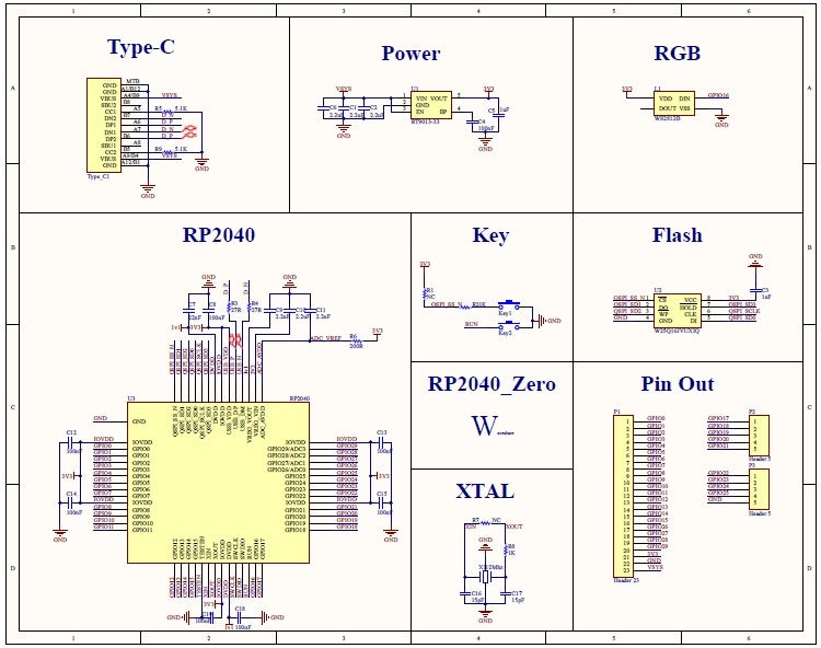
Schematic diagram for the RP2040 Zero .
Basic Programming Examples
The following MicroPython examples verify core functionality described in the RP2040 Zero datasheet. Flash either snippet using the Thonny IDE or drop a UF2 file via the BOOTSEL bootloader.
Test the onboard WS2812 RGB LED (GPIO16):
# MicroPython: Cycle the onboard WS2812 RGB LED on GPIO16
import machine, neopixel, time

np = neopixel.NeoPixel(machine.Pin(16), 1)
colors = [(255, 0, 0), (0, 255, 0), (0, 0, 255)]

for color in colors:
    np[0] = color
    np.write()
    time.sleep(0.5)
Running this confirms the microcontroller, onboard flash, clock, and GPIO16 are all operating correctly.
Read an analog voltage on ADC0 (GPIO26):
# MicroPython: Read analog voltage on ADC0 (GPIO26)
import machine

adc = machine.ADC(26)
raw = adc.read_u16()
voltage = raw * 3.3 / 65535
print(f"Voltage: {voltage:.2f} V")
This verifies the 12-bit ADC is functioning within the expected 0–3.3 V input range. Do not exceed 3.3 V on this pin.
Toggle a GPIO output using the Raspberry Pi Pico C SDK:
// C SDK: Toggle GPIO0 as a digital output
#include "pico/stdlib.h"

int main() {
    gpio_init(0);
    gpio_set_dir(0, GPIO_OUT);
    while (true) {
        gpio_put(0, 1);
        sleep_ms(500);
        gpio_put(0, 0);
        sleep_ms(500);
    }
}
Surface Mount Technology (SMT) Daughterboard Mounting on Carrier PCBs
The castellated holes along the edge of the RP2040 Zero allow the board to be surface-mounted directly onto a primary carrier PCB. Rather than manually tracing the castellated pad pattern, Ultra Librarian’s CAD model page provides a verified RP2040 Zero footprint ready to drop into your layout. When designing the host PCB footprint:
Maintain a 0.05 mm solder mask expansion around castellated pads to prevent solder bridging.
Define a keepout zone on top-layer copper underneath the RP2040 Zero to prevent exposed underside test pads from shorting against carrier traces.
Place ground thermal vias on the carrier PCB near Pin 2 and Pin 19 to help dissipate operational heat away from the MCU.
Hardware Troubleshooting and Debugging
Bootloader Recovery: If corrupt program code prevents USB enumeration, press and hold the onboard BOOTSEL button while connecting the USB-C cable. The board mounts as an RPI-RP2 mass storage volume, allowing a flash-clearing UF2 file to be dropped onto the drive to reset flash memory.
SWD Hardware Debugging: Serial Wire Debug pads (SWCLK, SWDIO, GND) are accessible on the underside of the PCB. Connecting an external hardware debugger (such as a Raspberry Pi Debug Probe) to these pads enables step-debugging and register inspection via hardware test points.
Power Rail Protection: Avoid supplying external power to the 3V3 pin while simultaneously plugging in USB-C power. Backfeeding voltage into the 3.3 V rail can damage the ME6211 LDO regulator. When powering external systems, connect power through the 5V input pin (Pin 1) and let the onboard regulator supply the 3.3 V rail.
PCB designers referencing the RP2040 Zero datasheet can access verified footprints, schematic symbols, and 3D STEP models for the RP2040 Zero and thousands of other components through Ultra Librarian, all formatted for your ECAD tool of choice. Register today for free.
Frequently Asked Questions
Is the RP2040 Zero 5V tolerant on its GPIO pins?
No. All GPIO pins on the RP2040 Zero operate strictly at 3.3 V logic levels. Exceeding 3.3 V on any digital or analog pin will degrade or destroy the RP2040 input buffer. Interfacing with 5V logic systems requires level-shifters.
How many GPIO pins does the RP2040 Zero expose?
The board exposes 29 GPIO pins in total. Twenty pins route to the dual 10-pin castellated headers along the perimeter, while nine additional GPIO pins connect to solder pads located on the underside of the board.
Does the RP2040 Zero include onboard Wi-Fi or Bluetooth?
No. The RP2040 Zero includes wired interfaces such as USB, SPI, I2C, UART, and PIO. Wireless networking requires connecting an external wireless module, such as an ESP32 or CYW43439 transceiver, via SPI or UART.
How is the onboard RGB LED connected on the RP2040 Zero?
The onboard WS2812 RGB LED connects internally to GPIO16. Controlling the LED requires generating an 800 kHz timing bitstream signal on GPIO16 using a software library or a PIO state machine.
What is the difference between Sleep mode and Dormant mode on the RP2040?
In Sleep mode, system clocks remain active while ARM CPU cores are halted, drawing approximately 1.3 mA. In Dormant mode, all internal system clocks and phase-locked loops (PLLs) are completely disabled, reducing power draw to approximately 180 µA until an external pin interrupt wakes the device.
Ultra Librarian offers the world’s largest PCB CAD library, putting cutting-edge materials at your fingertips so you can build better products faster—all for free.
Join Our Newsletter
Subscribe to our newsletter to receive the latest news, and important updates
If you’re looking for any of our component footprints or models, we have readily available and free options for you and your design team. Search our library for the solution you’ve been looking for.
Working with us allows you to target the right audience for your component, provide content to nurture them along their design process, and analyze how your parts are being received and used.
Ultra Librarian is the worlds largest online – and always free – PCB CAD library. Build products better, faster, and more accurately with easy access to vendor-verified symbols, footprints, and 3D models. Register today to start searching the right components for your next design.




 If you’re looking for any of our component footprints or models, we have readily available and free options for you and your design team. Search our library for the solution you’ve been looking for.