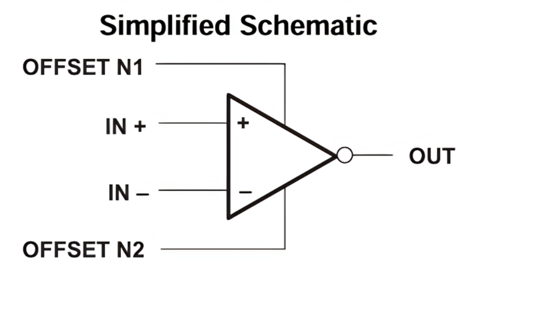
UA741CP operational amplifier schematic diagram with input, output, and offset pins.
The UA741CP Datasheet provides essential information about one of the most widely used operational amplifiers in electronics. It details the component’s specifications and electrical characteristics, helping engineers and students select and use it correctly in their circuits.
The datasheet also includes key parameters such as input offset voltage, supply current, slew rate, and open-loop gain. These characteristics allow users to evaluate the component’s suitability for various applications, including signal amplification, filtering, and analog computation. With clear tables and detailed data, the UA741CP datasheet simplifies design decisions and ensures reliable circuit performance.
UA741CP Datasheet Overview and Technical Details
The UA741CP’s performance is shaped by specific electrical limits that define how it functions in practical circuits. These details help engineers anticipate factors like accuracy, speed, and stability during design. Looking beyond the datasheet as a simple set of numbers, it reveals how the op-amp reacts to input signals, power supply variations, and external noise, which in turn supports the creation of dependable analog systems.
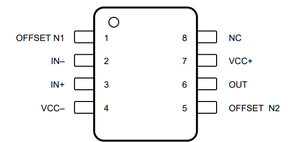
Standard 8-pin DIP layout of the UA741CP.
Internal Architecture
The internal architecture of the UA741CP is built around three main stages:
- Differential Input Stage: The first stage compares the inverting and non-inverting inputs and produces a differential current proportional to the voltage difference. This stage is directly connected to Pins 2 and 3 and determines input sensitivity and bias characteristics.
- Gain Stage: The amplified differential signal is then passed through a voltage gain stage, which significantly increases the signal magnitude. This stage ensures the high open-loop gain that makes the UA741CP suitable for precision amplification.
- Output Stage: Finally, the output stage delivers the signal to Pin 6, which is capable of driving resistive loads while maintaining stability. This stage also includes protective circuitry to safeguard the op-amp against overcurrent and short-circuit conditions.
Supporting circuitry, such as biasing networks and compensation capacitors, ensures stable operation across various frequencies and supply voltages.
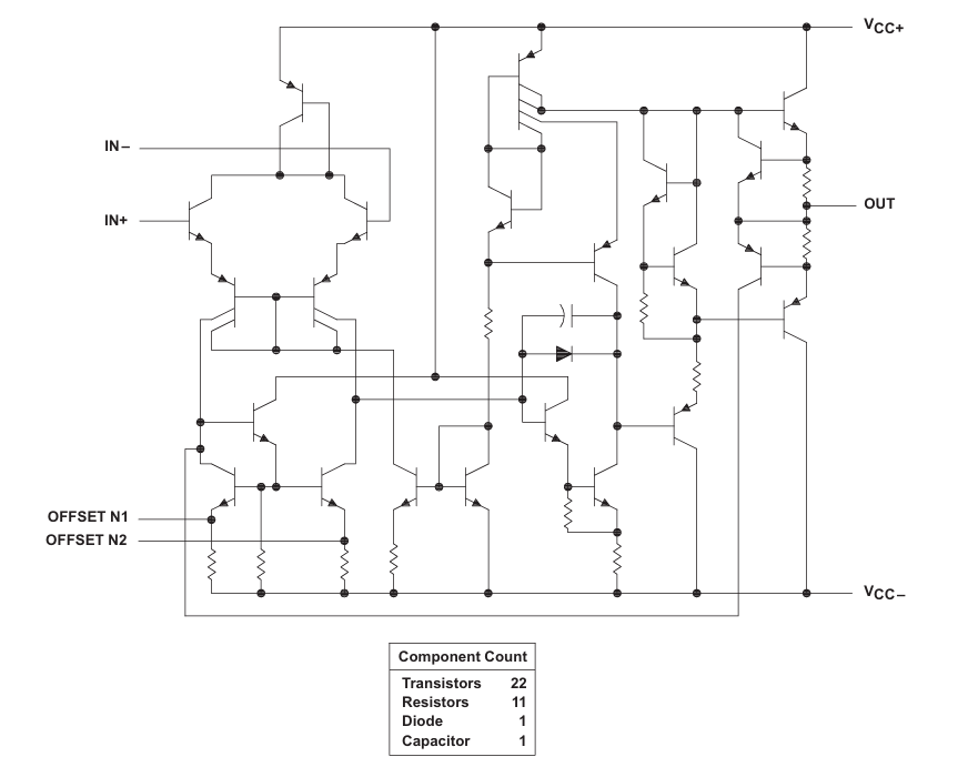
Internal block architecture of the UA741CP
Applications and Practical Usage of UA741CP
The UA741CP operational amplifier is highly versatile and can be used in a wide variety of analog circuits. Its combination of high open-loop gain, low input bias current, and stable operation makes it suitable for both educational projects and professional designs.
Whether used in signal conditioning or audio circuits, the UA741CP delivers predictable and stable performance. Its detailed datasheet, pin functionality, and versatile applications allow designers to implement circuits confidently and ensure reliable results across a wide range of analog designs.
To make implementation even easier, the UA741CP is available as CAD models compatible with common ECAD software. These include footprints, schematic symbols, and 3D models, which simplify simulation, layout verification, and integration into PCB designs. Platforms like Ultra Librarian provide downloadable files, allowing engineers to verify connections, plan layouts, and integrate the op-amp into complex designs before physically building the circuit.
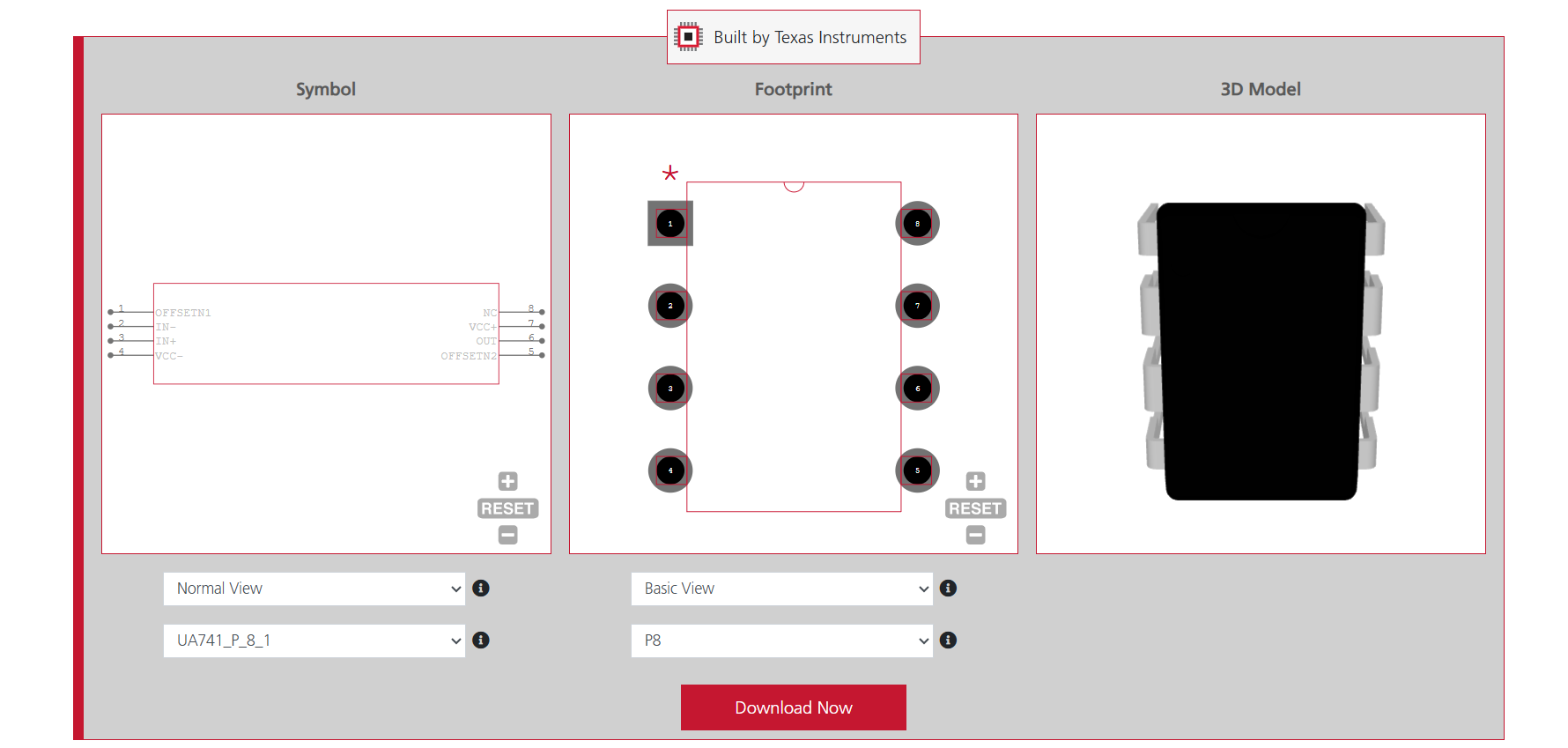
Schematic symbol, PCB footprint, and 3D model for the UA741CP
For access to CAD models for the UA741CP datasheet or other common components, Ultra Librarian compiles sourcing and design information in one place. Explore popular ECAD applications, connect with worldwide distributors, and see how working with Ultra Librarian streamlines design and production. Register today for free to access CAD files, schematic symbols, and footprints that help ensure error-free designs.


")
")