Releasing a printed circuit board to manufacturing without a thorough quality assurance evaluation will lead to expensive fabrication re-spins. Hardware engineers must systematically verify the physical layout against the original electrical design requirements. Implementing a standardized PCB design review checklist catches schematic discrepancies, signal integrity violations, and fabrication errors before releasing files to the factory floor.
The Core PCB Design Review Checklist
To streamline the quality assurance process, hardware teams can utilize the following table to track and complete each verification task prior to exporting final manufacturing files.
Production-Ready PCB Design Review Checklist
| Review Category | Verification Tasks |
| Schematic & BOM Parity | Verify zero unrouted nets. Confirm footprint assignments match the approved BOM exactly. |
| Stack-Up & Impedance | Confirm dielectric thickness, trace widths, and spacing rules achieve target controlled impedance. |
| High-Speed Routing | Ensure high-speed signals route over continuous, unbroken reference planes without crossing splits. |
| Power Distribution | Size power traces for expected current. Verify decoupling capacitors sit close to target IC pins. |
| Thermal Management | Apply thermal reliefs to pads on polygon pours. Ensure high-power components have adequate heat dissipation vias. |
| DFM & Clearances | Check component-to-component physical clearance, drill sizes, annular rings, and solder mask expansion limits. |
Schematic-to-Layout Parity and BOM Verification
The quality assurance process begins by confirming the physical layout accurately reflects the schematic logic.
LVS and DRC Execution
Electrical connections must pass a final Layout Versus Schematic (LVS) check and Design Rule Check (DRC). Engineers must:
- Verify zero unrouted nets exist in the database.
- Clear all outstanding DRC physical and electrical violations.
- Ensure all custom components map to the correct schematic symbol pins.
Footprint and BOM Cross-Referencing
Additionally, hardware teams must cross-reference the physical layout against the Bill of Materials (BOM). This verification ensures every assigned footprint matches the exact manufacturer part number. A mismatched footprint, such as placing an 0805 pad for a 0603 physical component, can cause an assembly failure on the factory line.
Stack-Up and High-Speed Routing Review
Modern hardware requires careful control of electromagnetic emissions and signal timing because high-speed switching can create interference, degrade signal integrity, and cause failures during operation or regulatory testing.
Impedance Control and Reference Planes
Evaluating the board stack-up involves confirming dielectric materials, copper weights, and layer assignments to ensure proper impedance control. For high-speed signals, engineers must trace the routing path to verify sensitive lines maintain a continuous reference plane. Routing high-speed traces over gaps or splits in the ground plane creates severe impedance discontinuities and return-path inductance.
Differential Pair Tuning
Hardware engineers must also verify the two traces in each differential pair are matched closely enough in electrical length to satisfy the allowable timing-skew tolerance. They should confirm any length-tuning meanders are placed near the location where the mismatch occurs, so the correction does not introduce unnecessary discontinuities or degrade signal integrity.
Power Distribution Network (PDN) and Thermal Management
A stable power distribution network prevents voltage droop and high-frequency noise from disrupting active components.
Power Traces and Decoupling
The engineering review must confirm power planes and trace widths provide adequate current-carrying capacity based on maximum expected thermal rise. Decoupling capacitors require placement immediately adjacent to integrated circuit power pins, utilizing short and wide traces to minimize parasitic loop inductance.
Thermal Relief Connections
Furthermore, engineers must verify thermal relief connections on all component pads tied to large copper pours. Without proper thermal reliefs, a pad tied directly to a copper pour can pull heat away faster than the reflow process can replace it, preventing said joint from reaching full reflow temperature and causing a cold solder joint.
On small two-terminal components, this uneven heating between pads (one pad connected to a thermal-relief spoke, the other tied solidly to a pour) can also cause tombstoning, where the component lifts and rotates onto the reflowed pad first.
Design for Manufacturability (DFM) Validation
A design might function perfectly in a software simulation while remaining physically unmanufacturable. Therefore, completing a rigorous PCB design review checklist requires DFM validation to ensure the layout adheres to the physical tolerances of the contract manufacturer, guaranteeing a reliable transition from design to production.
Core DFM Verification Steps
Engineers must verify the following constraints before manufacturing handoff:
- Trace clearances meet minimum fabrication limits to prevent electrical shorts.
- Minimum drill hole sizes and annular rings provide enough copper to prevent drill breakout.
- Solder mask dams between fine-pitch pins meet minimum assembly requirements to prevent solder bridging.
- Silkscreen ink avoids overlapping exposed copper pads, ensuring clean solder joints.
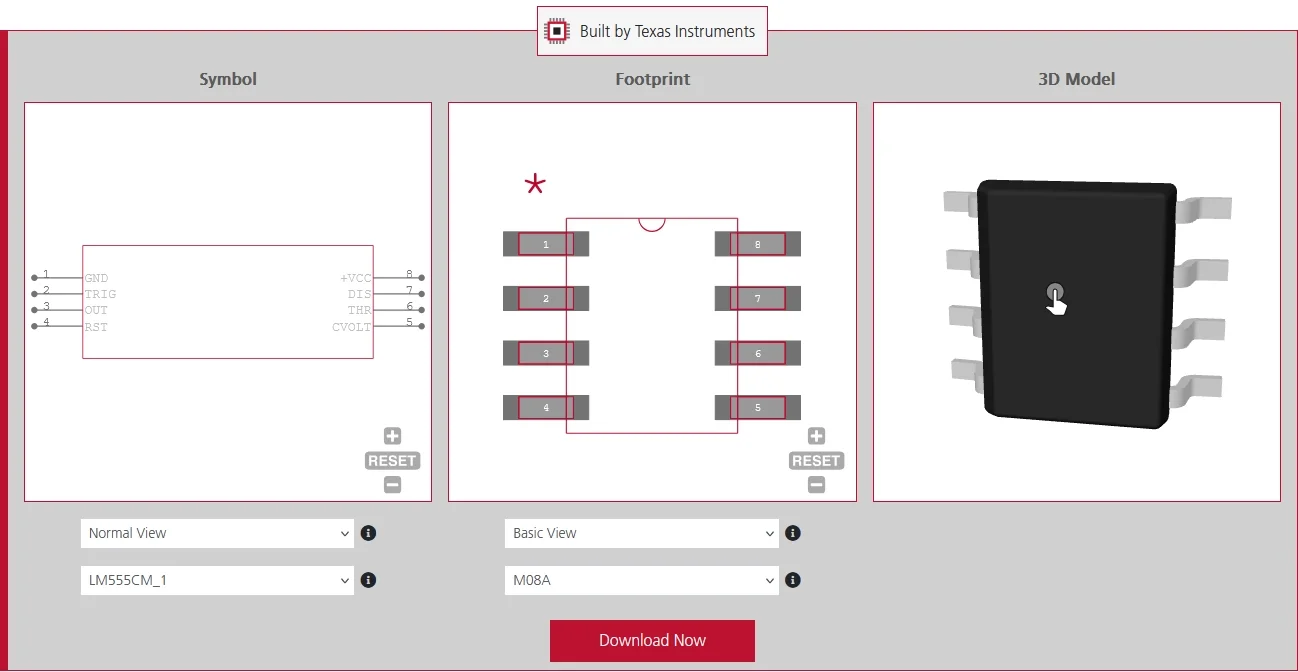
Sourcing reliable CAD models forms the foundation of any successful hardware project. Rather than building and verifying custom footprints from scratch, engineers can download verified schematic symbols and 3D models directly from Ultra Librarian in many popular ECAD applications.
Simplify your next PCB design review checklist with parts you can trust. Working with Ultra Librarian sets your team up for success, ensuring streamlined and error-free design, production, and sourcing. Register today for free.


 If you’re looking for any of our component footprints or models, we have readily available and free options for you and your design team. Search our library for the solution you’ve been looking for.