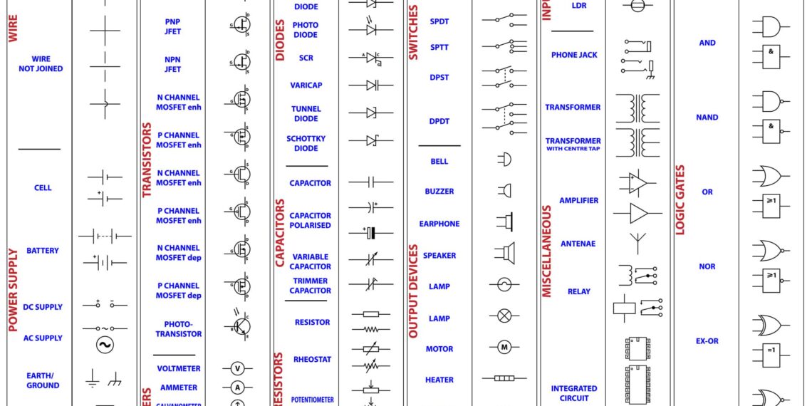
Think of electronic schematics as the blueprints every hardware design runs on, and basic electronic symbols as the language you need to read them. Without that fluency, turning a circuit idea into a working printed circuit board (PCB) is a lot harder than it needs to be. Every symbol pin connects directly to a physical footprint pad and a bill of materials (BOM) line item, so getting the symbols right is not optional. One wrong symbol can send errors downstream fast, quietly stacking up costly manufacturing delays. In this guide, we break down the essential schematic symbols every PCB designer needs to know.
Basic Electronic Symbols Standards
There are two main standards governing schematic symbols, and mixing them on the same schematic creates the kind of ambiguity that layout engineers and test technicians have to untangle manually.
IEC 60617:2025 (also known as BS 3939) is the current international standard for electronic symbols. Parts 2 through 13 cover a database of roughly 1,900 standardized graphical symbols. IEC 60617 represents components as rectangular blocks; a resistor, for example, shows up as an open rectangle with labeled terminals. If you’re reviewing European schematics, multinational hardware specs, or modern global design files, this is the standard you’ll run into.
IEEE 315-1975 (also known as ANSI Y32.2-1975) introduced the traditional North American symbols you probably know well, including the familiar zigzag resistor. The standard was reaffirmed in 1993, then officially inactivated on November 7, 2019, with no formal replacement issued for the U.S. market. That said, IEEE 315 symbology is still the go-to in North American EDA (Electronic Design Automation) tool libraries and most domestic engineering documentation.
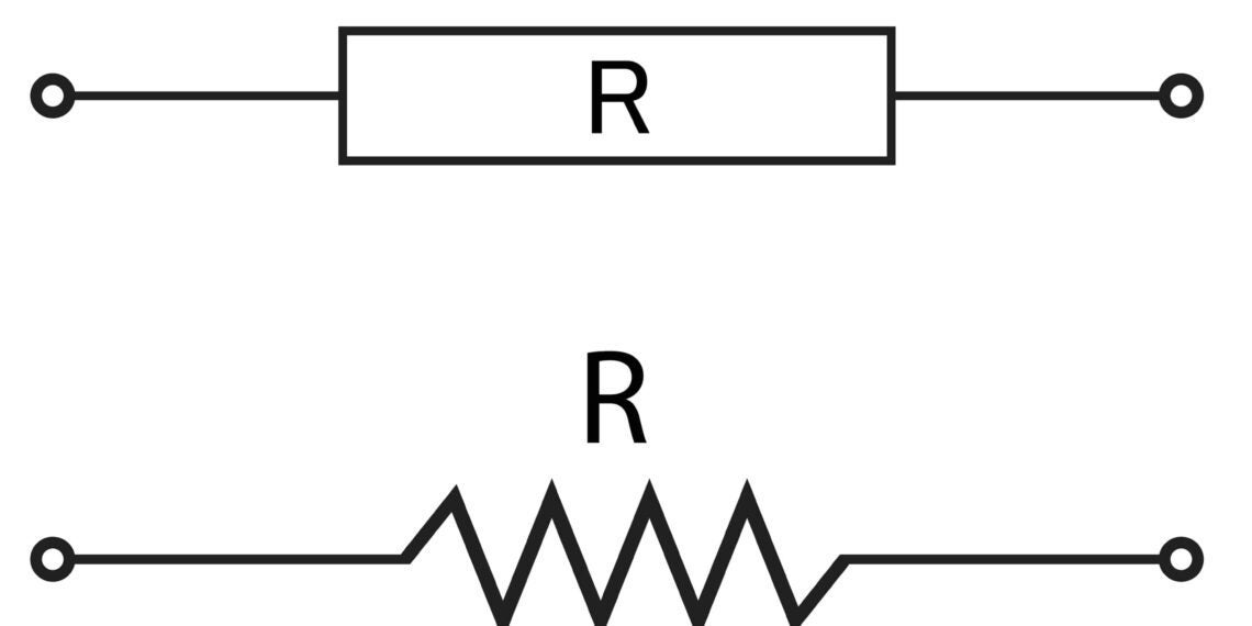
Resistor symbol in IEC 60617 vs IEEE 315
Passive Components: Resistors, Capacitors, and Inductors
Passive components regulate power and filter signals without needing an external power source.
- Resistor (R): Shown as a zig-zag line (IEEE) or an open rectangle (IEC). Add a diagonal arrow across the symbol, and you’ve got a variable resistor or potentiometer.
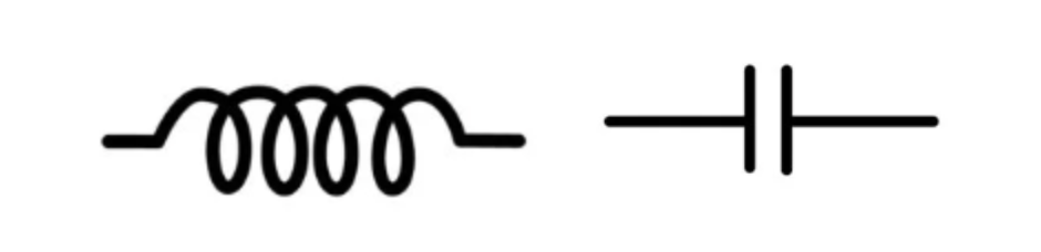
- Capacitor (C): Non-polarized capacitors use two parallel lines of equal length. Polarized capacitors (electrolytic or tantalum) mark the positive terminal with a “+” or pair a straight line with a curved negative plate. Reversing a polarized capacitor symbol in a schematic leads to reverse-bias installation; at power-up, the component will vent or rupture.
- Inductor (L): Shown as a series of connected semicircles (IEEE) or a filled rectangle (IEC). You’ll see inductors a lot in switching power supply schematics, where their value and saturation current rating really matter.
Active Components: Diodes, Transistors, and ICs
Active components need external power to operate and control current direction or magnitude. The symbol geometry encodes polarity directly, so misreading one here can actually flip the intended function.
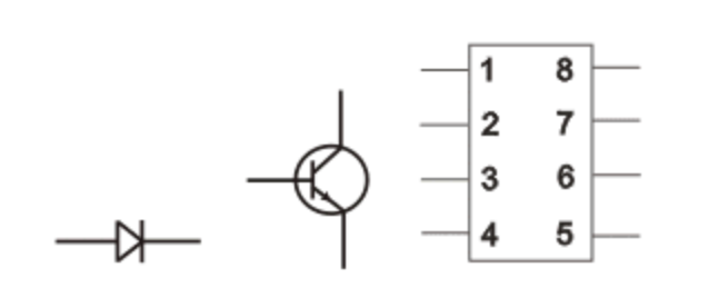
- Diode (D): A triangle pointing toward a perpendicular line. The triangle’s flat base is the anode; the line is the cathode. The triangle points in the direction of conventional current flow. Reversing the symbol completely blocks the intended signal path.
- Transistor (Q):
- Bipolar Junction Transistors (BJTs) are drawn with three terminals: base, collector, and emitter. The arrow on the emitter indicates the current direction: pointing outward for NPN (Negative-Positive-Negative) and inward for PNP (Positive-Negative-Positive).
- Metal-Oxide-Semiconductor Field-Effect Transistors (MOSFETs) are drawn with three terminals: gate, drain, and source. The symbol features a visible gap between the gate and the conductive channel to represent electrical isolation. MOSFET symbols often include an internal body diode spanning the drain and source, which becomes relevant in synchronous rectification and electrostatic discharge (ESD) protection designs.
- Integrated Circuit (U): Complex ICs use rectangular blocks with numbered pins along the perimeter. Pin 1 is always explicitly marked, usually with a dot or a chamfered corner, to maintain correct orientation during pick-and-place assembly. A missing Pin 1 marker is one of the most common causes of component rotation errors.
Power, Ground, and Connectivity Symbols
Ground and power connections are the backbone of any schematic, routing supply voltages and return paths throughout the design.
Standard Ground and Power Symbol Reference
| Symbol Type | Graphical Representation | Function |
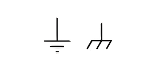
| Earth Ground | Three horizontal lines of decreasing width, pointing downward | Connects the circuit to physical earth; used for safety fault current return |
| Chassis Ground | A vertical line connecting to three angled parallel lines | Indicates connection to the metal enclosure or mechanical frame |
| Signal Ground | A hollow triangle pointing downward | Defines the 0 V reference for digital or analog signals on the PCB |
| Power Node (VCC/VDD) | An arrow, circle, or bar pointing upward, labeled with a voltage | Ties a node to a named supply rail without drawing individual routing lines across the sheet |
Wire junctions use a solid dot where two lines cross. No dot means the traces pass through each other without an electrical connection. Miss a required junction dot, and you’ll leave component pins floating, which usually won’t show up until continuity testing after the board is already assembled.
From Schematic Capture to PCBA
Every schematic symbol leads to a physical part on the finished board.
- Modern EDA tools link each graphical symbol to a specific land pattern and a 3D mechanical model within a component library.
- When the schematic is compiled, the software generates a netlist: a plain-text file that maps every symbol pin to an exact PCB footprint pad (for example, Symbol U1 Pin 4 connects to Symbol C2 Pin 1).
- The PCB layout tool imports that netlist and places the assigned footprints on the board canvas.
Once the software populates the board canvas, the physical dimensions of those components take over. The footprint dimensions are not arbitrary: IPC-7351C sets requirements for land-pattern geometries used in surface-mount technology (SMT) and provides recommendations for optimal solder joints. Rather than locking in fixed pad dimensions, the standard uses mathematical algorithms to calculate optimal pad sizes based on component dimensions, manufacturing tolerances, and desired solder fillet goals.
Assign the wrong footprint (say, an 0402 land pattern on a component specified as 0805 in the BOM), and the assembly machine simply won’t be able to place the part. IPC-7351C covers land pattern design across passive and active component families: resistors, capacitors, MELFs, SOPs, QFPs, BGAs, QFNs, and SONs. Follow these guidelines, and your accurate symbols will carry the intended design all the way through to manufacturable hardware.
Schematic Reading Tips for Layout Engineers
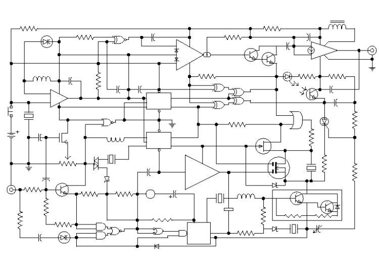
Before starting layout on a new schematic, run through these checks in order:
- Confirm the symbol standard in use. Check the title block or library notes. If IEEE and IEC symbols are mixed, flag them before you import the netlist.
- Verify all polarized component orientations. Cross-reference the positive terminal marker on every capacitor and diode symbol against the net names (e.g., VCC vs. GND) on adjacent pins.
- Audit every wire junction. A missing dot on a four-way intersection is one of the hardest defects to catch visually. Use your EDA tool’s ERC (Electrical Rules Check) to flag unconnected pins.
- Check Pin 1 markers on all ICs. Confirm Pin 1 on the symbol matches the physical Pin 1 indicator on the component datasheet before assigning the footprint.
- Validate supply rail names. A net named “3V3” on one sheet and “3.3V” on another won’t short in the netlist. They become two completely separate, unconnected rails.
Getting basic electronic symbols right is the first step to a clean board spin. There’s no good reason to build your own CAD assets from scratch and risk downstream translation errors that make their way into your layout.
Working with Ultra Librarian sets your team up for success, ensuring streamlined and error-free design, production, and sourcing. Register today for free.

 If you’re looking for any of our component footprints or models, we have readily available and free options for you and your design team. Search our library for the solution you’ve been looking for.