The CD74HCT20E Datasheet provides essential design information for this popular IC.
When designing digital circuits, it is important to understand the symbols and functionality of common gate symbols, like the NAND or “NOT AND” gate. NAND gates are implemented in various types of digital devices and circuits, including arithmetic logic units (ALUs), decoders, encoders, and multiplexers. The popularity of these logic gates is derived from the fact that they can be used to create virtually any logic function or operation. In fact, it is not unusual to find entire circuits composed of only NAND gates. Most often, NAND gates come in IC packages consisting of multiple components. A good example of this is the CD74HCT20E datasheet, which includes essential design information for effectively implementing a DUAL NAND gate architecture.CD74HCT20E: Features and Applications
From the CD74HCT20E datasheet, the versatile dual NAND gate component has the following features:In addition to the electrical characteristics above, the CD74HCT20E datasheet also informs the device operates reliably across industrial temperature ranges (-40°C to +85°C) and provides TTL-compatible input thresholds while maintaining CMOS power efficiency. This makes it ideal for mixed-signal designs where legacy TTL interfaces must communicate with modern CMOS circuitry.
CD74HCT20E: Pinout and Pin Descriptions
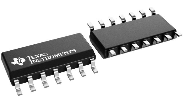
The CD74HCT20E pinout is shown below.
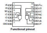
The pinout of the CD74HCT20E
As shown, the chip contains two 4-input NAND gates conveniently located on opposite sides of the IC package. The two independent 4-input NAND gates share common power and ground connections. All of the pin functions are listed below.
Critical Connection Notes:
Unused inputs must be tied to VCC or GND to prevent floating states
Power supply decoupling requires a 0.1 µF ceramic capacitor between VCC and GND
Output loading should not exceed 4.0 mA sink or source current per gate
Input protection includes internal diode clamps to VCC and GND
CD74HCT20E: Operation and Circuit Example
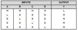
The CD74HCT20E performs standard Boolean algebra AND operations between the four inputs. This results in the logic diagram for each gate below. NOTE: X indicates “Don’t Care” connections that have no effect on device operation.
Functional Diagram for CD74HCT20E NAND gates
The CD74HCT20E serves multiple functions in digital systems, from basic logic operations to complex timing circuits. Below, a common application of the device used to perform SR latch functionality is shown.
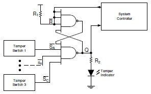
Example CD74HCT20E implementation
Alternative Components to the CD74HCT20E
There may be situations where using the CD74HCT20E is not a viable option. For example, if the device is not reliably available due to supply chain issues or is cost-prohibitive due to market fluctuations. A PCB design best practice for a robust component library is to compile a list of practical alternatives, as listed below, for the CD74HCT20E.
Using an alternative component is always a compromise and weighing the trade-offs should drive your final selection. Below are some tips for alternative selection, if necessary, to replace the CD74HCT20E.
CD74HCT20E Replacement Tips:
- For power-sensitive designs
Choose 74HC20 for battery-powered applications
- For legacy TTL compatibility
Stick with HCT variants for 5 V systems
- For a wide voltage range
Consider CD4012B for 3 V to 18 V operation
- For high-speed applications
Evaluate 74LS20 for sub-10 ns propagation delays
PCB Design with the CD74HCT20E Datasheet
Effective PCB design with the CD74HCT20E dual 4-input NAND gate begins with having accurate and comprehensive data and information. The CD74HCT20E datasheet is an essential source that provides much of the necessary design resources. However, it is also critical that you acquire and use an accurate schematic symbol, PCB footprint, and 3D CAD model (especially, for ECAD-MCAD designs), as shown below.
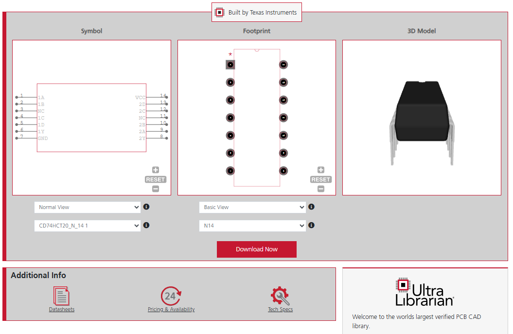
Schematic symbol, PCB footprint, and 3D CAD model of the CD74HCT20E from UL
Failing to do so will lead to inaccuracies in your schematic and layout, which can derail the building of your boards. To avoid these potential contingencies, you should always source CAD models and datasheets from trusted sources.
If you’re looking for CAD models for common components or important information for creating the best design from the CD74HCT20E datasheet, Ultra Librarian helps by compiling all your sourcing and CAD information in one place.
Working with Ultra Librarian sets up your team for success to ensure streamlined and error-free design, production, and sourcing. Register today for free.