
When a signal frequency exceeds roughly 100 MHz, a copper trace stops behaving like a wire and becomes a transmission line. At that point, the physical geometry of the trace, not its DC resistance, governs how much signal energy reaches the receiver and how much bounces back toward the source. That’s the core problem PCB impedance control solves.
Characteristic impedance, measured in ohms, describes the ratio of voltage to current in a propagating wave along the transmission line. When the source, trace, and load impedances are matched, energy transfers cleanly. When they’re not, reflections occur. Those reflections manifest as voltage ringing, waveform distortion, and collapsed noise margins that cause bit errors in digital systems and measurement errors in analog ones. Uncontrolled mismatches also turn traces into unintentional antennas, generating radiated EMI that can sink a regulatory compliance test.
Industry-Standard Impedance Targets
Hardware designers don’t pick impedance targets arbitrarily. The physical layer (PHY) specification for each communication standard defines the target, and your PCB traces must match it to work with off-the-shelf transceivers, cables, and connectors.
| Protocol | Signal Type | Target Impedance | Tolerance |
| General RF / Antenna | Single-Ended | 50 Ω | ±10% |
| DDR Memory (data lines) | Single-Ended | 40–50 Ω | ±10% |
| USB 2.0 / 3.x | Differential | 90 Ω | ±15% |
| PCIe (all generations) | Differential | 85 Ω | ±10% (tighter for Gen 5) |
| Gigabit Ethernet | Differential | 100 Ω | ±10% |
A few notes on these values that trip up designers: USB 2.0 and USB 3.x both require a differential impedance of 90 Ω ±15%, though the ±10% figure is commonly cited in board-level design guides as a more conservative working target. For PCIe, the target differential impedance for PCI Express lanes is 100 Ω ±10%, as required by the PCI-SIG. However, 85-ohm differential impedance is the PCI-SIG recommended impedance for trace routing, reflecting a deliberate mismatch between the trace impedance and the 100 Ω termination resistors at the die. The PCIe spec accommodates this by allowing a range; for add-in cards specifically, 85 Ω differential impedance is the requirement. When in doubt, check the CEM specification for your specific topology.
What Actually Controls Trace Impedance
Characteristic impedance is determined entirely by the cross-sectional geometry of the trace and the electrical properties of the surrounding dielectric, not by the trace’s length or DC resistance. Get the geometry right, and you control impedance. Get it wrong, and no amount of careful routing will save you.
Trace Width, Copper Thickness, and Differential Spacing
Wider traces provide more capacitance to the reference plane, lowering impedance. Thicker copper does the same. Both relationships are inversely proportional: increasing the width or thickness decreases impedance. This is why narrow traces on outer layers tend to have higher impedance than wide traces on inner layers with the same dielectric height.
For differential pairs, the spacing between the two conductors adds a third variable. Tighter coupling (closer spacing) lowers the differential impedance; wider spacing raises it.
Two manufacturing realities matter here:
- Etch tolerance: Standard fabrication processes hold trace width to roughly ±1 mil. On a 4-mil trace, that’s a 25% dimensional variation, which translates directly into a significant impedance swing. Narrow controlled-impedance traces require tighter process control and often cost more.
- Copper weight and etch quality: When copper thickness reaches 3 oz or higher, etching efficiency decreases, and a larger minimum trace width is required. Conventional etching techniques are not ideal for manufacturing heavy copper PCBs, as they produce over-etched edges and uneven edge lines. For impedance-controlled signal layers, 1 oz copper is standard; for high-frequency designs above 1 GHz, ≤1 oz copper is preferred to minimize skin-effect losses.
Dielectric Constant and Stack-Up Geometry
The substrate separating a signal trace from its reference plane acts as a capacitor dielectric. Two material properties govern the impedance:
Dielectric thickness (H) is directly proportional to impedance. Move the trace further from its reference plane, and impedance rises. Compress the dielectric, and it falls. This is why stack-up geometry is not only a mechanical decision, but also an electrical one.
Dielectric constant (Dk, or relative permittivity Eᵣ) is inversely proportional to impedance. Higher Dk materials produce lower impedances at the same geometry.
Standard FR-4 has a Dk that fluctuates with frequency and temperature, making it harder to maintain precise impedance targets at multi-gigabit speeds. Once PCIe Gen 4 came out, FR-4 was no longer the best option, and lower-loss laminates were needed to support routing over the distances found in a rackmount unit or a motherboard. For these designs, specify low-loss laminates (Rogers, Megtron 6, and similar materials) that offer stable Dk and low loss tangent across the frequency range of interest.
Simulation Tools: What Fabricators and Designers Actually Use
Calculating the impedance of microstrip (outer-layer) and stripline (inner-layer) structures analytically requires solving electromagnetic field equations. In practice, everyone uses software.
Fabrication Industry Tools
The industry reference tools come from Polar Instruments, primarily:
- Si8000m
- Lossless impedance prediction
- Used for stack-up verification
- Si9000e
- Frequency-dependent transmission line modeling
- Uses the boundary element method for field solving
- Extracts RLGC matrices
- Models the conductor, dielectric, and insertion loss
- Preferred for multi-gigabit channel analysis
- Continues to be actively developed with expanded transmission line structures
Design-Side (EDA) Tools
On the design side, PCB engineers work inside their EDA platforms. For example, Altium Designer’s layer stack manager with its integrated field solver, or Cadence Allegro with Sigrity, to:
- Input a target impedance (e.g., 50 Ω, 90 Ω diff)
- Dynamically calculate required trace widths and spacing
- Adjust geometry during layout
These tools use the same field-solving mathematics but differ in how they integrate directly into the PCB workflow.
Critical Routing Rules for Impedance-Controlled Nets
A perfectly modeled stack-up will fail in the field if routing discipline breaks down. Impedance is controlled only where the trace’s physical environment is uniform.
Follow these rules on every impedance-controlled net:
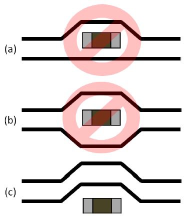
- Never route over a split plane. Your trace requires a continuous, uninterrupted reference plane directly beneath or above it. Routing SuperSpeed traces over a split in the reference plane kills signal return paths. The same principle applies to every high-speed net, not just USB.
- Keep differential pair spacing constant. Using inconsistent trace spacing or width — for example, due to uneven via pads or solder mask — can push impedance out of tolerance. Route the pair as a coupled unit through the entire channel.
- Minimize layer transitions. Every via introduces a parasitic inductance-capacitance discontinuity. When a layer change is unavoidable, place a ground return via immediately adjacent to the signal via to maintain a continuous return current path. The signal via effectively reduces the allowable channel length by approximately 2 inches; if a layer change is required, always place a ground via flanking the signal via to maintain the ground return path.
How Your Fabricator Hits the Target
When your Gerber files arrive at the fab house, the manufacturer doesn’t simply print your nominal trace widths. They run their own pre-production analysis, because they know something you don’t: exactly how their chemistry and materials behave on their specific process line.
The fabricator imports your stack-up into their field solver and applies micro-corrections to trace widths and spacings based on their known etch bias. They also recalculate dielectric assumptions, because the theoretical thickness of a prepreg sheet on a datasheet rarely matches its final pressed-and-cured thickness. This is why your fabrication notes should specify your electrical target (e.g., “50 Ω ±10%, single-ended, Layer 2 microstrip”) rather than locking in a specific trace width. Locking width removes the fabricator’s ability to compensate.
PCB Impedance Control Verification with TDR Test Coupons
Once boards are manufactured, the fabricator must prove that the targets were met. Fabricators rarely test functional traces directly because:
- Component pads create discontinuities
- Vias introduce parasitics
- Routing bends distort the measurement
Instead, fabricators use test coupons – small PCBs approximately 200x30mm with the same layer and trace construction as the main PCB. More specifically, impedance test coupons are:
- Straight transmission-line structures
- Placed on the outer edges of the same production panel
- Built using the identical lamination and etch cycle
Because test coupons mirror the controlled-impedance structures on your PCB, they provide accurate verification. In testing, fabricators use a test instrument known as a Time-Domain Reflectometer (TDR), which:
- Launches a fast-rise-time voltage step
- Measures reflected waveform amplitude
- Maps reflected-to-incident voltage ratio to impedance along the trace (e.g., test coupons)
- Produces a spatial impedance profile
If the coupon passes, the boards on that panel are guaranteed to meet your specification.
Now that you understand the critical factors driving PCB impedance control, the next step is to source the right components with accurate CAD models that match your stack-up. Ultra Librarian gives you access to verified symbols, footprints, and 3D models for popular ECAD applications and connects you to worldwide distributors so you can confidently design high-speed channels that work on the first spin.
Working with Ultra Librarian sets your team up for success, ensuring streamlined and error-free design, production, and sourcing. Register today for free.