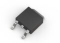
Universal Serial Bus (USB) ports take a hit from electrostatic discharge (ESD) whenever a charged person, cable, or peripheral touches the interface. Because the connectors provide ESD with a direct path into the printed circuit board (PCB), protection should be placed close to the connector, where it diverts transients before they reach the USB transceiver.
The STMicroelectronics USBLC6-2SC6 is a transient voltage suppressor (TVS) array with two protected data channels plus VBUS protection in a SOT-23-6 package. The USBLC6-2SC6 datasheet specifies International Electrotechnical Commission (IEC) 61000-4-2 level 4 protection for ±15 kV air discharge and ±8 kV contact discharge, and its low line capacitance supports USB 2.0 high-speed data rates up to 480 Mb/s. This combination has made it a widely used protection device for USB 2.0 designs.
USBLC6-2SC6 Datasheet: ESD Protection and Electrical Specs
The USBLC6-2SC6 protects USB 2.0 interfaces from electrostatic discharge. The device connects to the D+, D-, VBUS, and ground paths near the USB connector. During normal operation, the low-capacitance protection network has minimal effect on the USB data signals. During an ESD event, the TVS structure redirects transient current away from the USB transceiver and into the supply or ground path.
The USBLC6-2SC6 datasheet specifies the following:
- Two protected data channels
- Protection for the 5 V VBUS rail
- 2.5 pF typical and 3.5 pF maximum capacitance from an input/output (I/O) pin to ground
- Suitability for USB 2.0 data lines, with a low-capacitance load on the D+ and D- differential pair
- Preserved signal quality at 480 Mb/s
USBLC6-2SC6 Electrical and ESD Specifications
| Specification | USBLC6-2SC6 Value |
| Air discharge protection | ±15 kV |
| Contact discharge protection | ±8 kV |
| Reverse stand-off voltage | 5.25 V |
| Breakdown voltage | 6 V min. |
| Clamping voltage at 1 A (8/20 µs) | 12 V max. |
| Clamping voltage at 5 A (8/20 µs) | 17 V max. |
| I/O to GND capacitance | 2.5 pF typ., 3.5 pF max. |
| I/O to I/O capacitance | 1.2 pF typ., 1.7 pF max. |
| Operating junction temperature | -40 °C to 150 °C |
| Package | SOT-23-6 |
Clamping voltage rises with transient current. PCB trace inductance can increase the voltage seen by the protected circuit, so device placement and grounding affect ESD performance as much as component selection. Both clamping values are specified on the 8/20 µs surge waveform, so compare any alternative at the same pulse current and waveform.
USBLC6-2SC6 Pinout and SOT-23-6 Package
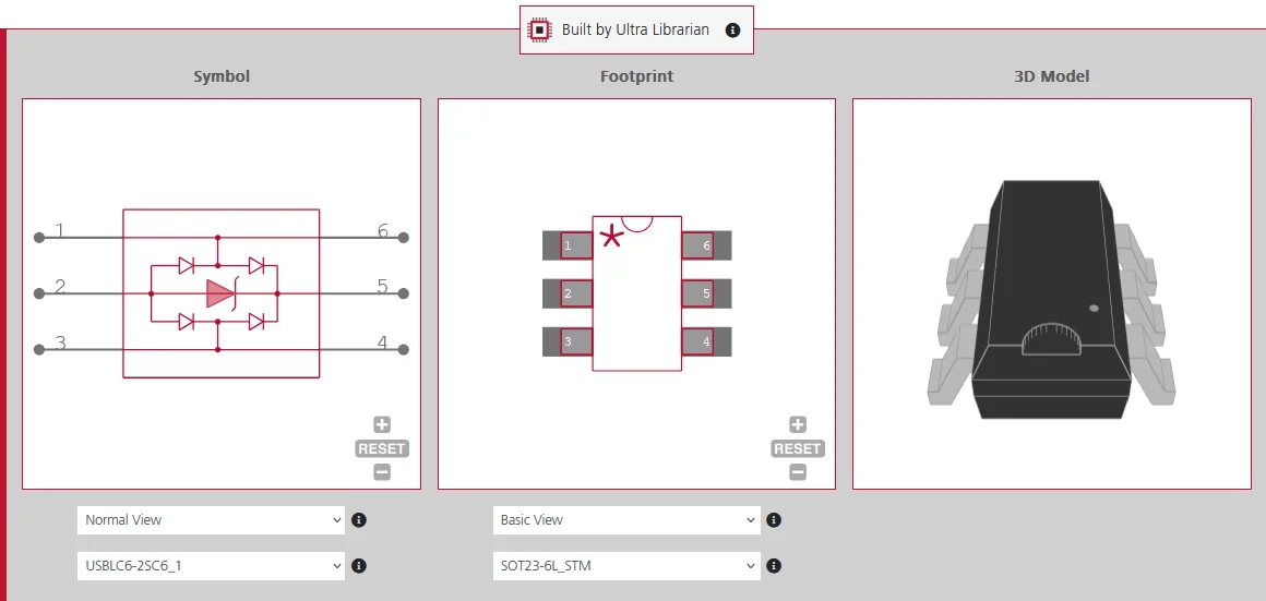
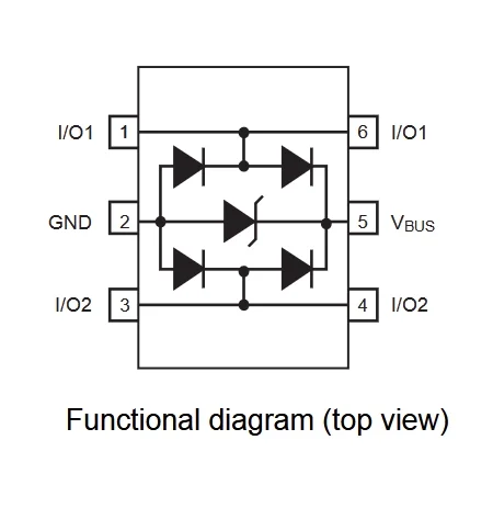
The USBLC6-2SC6 pinout uses paired pins for two bidirectional data channels. Pins 1 and 6 form I/O1, while pins 3 and 4 form I/O2. Pin 2 connects to ground, and pin 5 connects to VBUS.
USBLC6-2SC6 Pinout and USB 2.0 Connections
| Pin | Function | Connects to |
| 1 | I/O1 | D+ from the connector |
| 2 | GND | Ground plane |
| 3 | I/O2 | D- from the connector |
| 4 | I/O2 | D- to the transceiver |
| 5 | VBUS | USB 5 V rail |
| 6 | I/O1 | D+ to the transceiver |
Because the data channels are bidirectional, the two pins in each pair are interchangeable as input and output. Package orientation still matters because GND and VBUS use dedicated pins.
USB 2.0 PCB Layout and ESD Protection
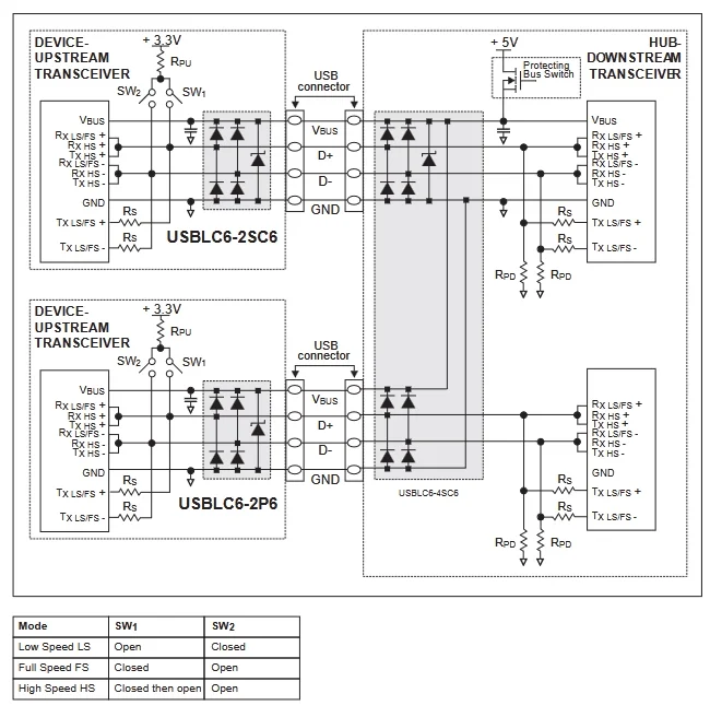
PCB placement directly affects ESD protection. In a typical USBLC6-2SC6 application circuit, the device sits between the USB connector and the USB transceiver, with D+ and D- routed through its protected I/O channels and VBUS connected to the supply pin.
The USBLC6-2SC6 should therefore sit as close as practical to the USB connector. Connections between the connector and the TVS array should stay short. The ground connection should use a short path to a low-impedance ground plane, since extra trace length adds parasitic inductance, which can increase the transient voltage during a fast ESD event.
A clean layout routes D+ and D- straight through the paired I/O pins. Common layout mistakes include:
- Placing the USB ESD protection diode too far from the connector
- Using a long or narrow ground return path
- Rotating or mirroring the footprint without checking the GND and VBUS pin locations
- Routing exposed connector-side traces close to protected circuitry
Ultra Librarian’s computer-aided design (CAD) model standards can help verify symbols and footprints before layout. The STMicroelectronics component library also provides CAD data for related parts.
Selecting a USBLC6-2SC6 Equivalent
A USBLC6-2SC6 equivalent needs more than the same SOT-23-6 package. Check each of these against the requirements of the USB interface:
- Pin mapping: I/O, GND, and VBUS locations match the USBLC6-2SC6 pinout
- Reverse stand-off voltage: above the 5 V VBUS rail
- ESD rating: meets the protection level the design requires
- Capacitance: low enough for D+ and D- at 480 Mb/s
- Leakage current: acceptable for the application
- Clamping voltage: compared at the same pulse current and 8/20 µs waveform
Capacitance deserves close attention. A pin-compatible device can still impose excessive loading on D+ and D-. An alternative intended for USB 2.0 should provide capacitance suitable for a 480 Mb/s differential interface. The USBLC6-2SC6 is specified for USB 2.0 high-speed operation rather than USB 3.x SuperSpeed signaling. USB 3.x interfaces retain a separate D+/D- pair for USB 2.0 compatibility. Their SuperSpeed transmit and receive pairs operate at much higher data rates and require ESD protection characterized for those lines.
A clamping voltage measured at one pulse current should not be compared directly with one measured under a different waveform or current level.
USBLC6-2SC6 CAD Models for PCB Design
The USBLC6-2SC6 has historically been one of Ultra Librarian’s most-downloaded components. Accurate CAD data helps keep the schematic symbol, SOT-23-6 footprint, pin mapping, and package geometry consistent with the USBLC6-2SC6 datasheet.
Download the USBLC6-2SC6 symbol, footprint, and 3D model from Ultra Librarian to add verified CAD data directly to your PCB design workflow.
Keep your design in line with the USBLC6-2SC6 datasheet: register today to get free, verified CAD models from Ultra Librarian, built for PCB designers.

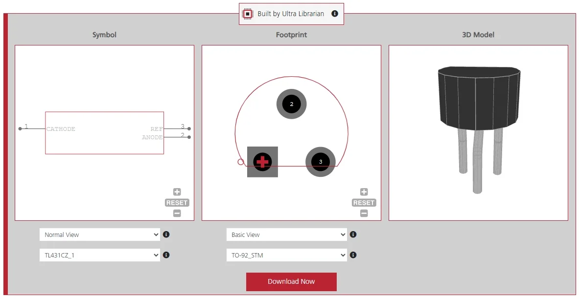
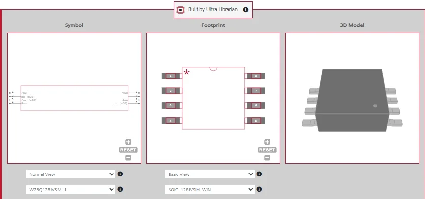
 If you’re looking for any of our component footprints or models, we have readily available and free options for you and your design team. Search our library for the solution you’ve been looking for.