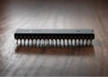
The ATmega328P is available in standard packages like QFP
The ATmega328P is an 8-bit AVR microcontroller chip developed by Atmel, but is now produced by Microchip Technology, Inc. A common component in Arduino robotics, the device is known for high performance with low power consumption. Designed for very high processing speeds, the ATmega328P includes many special features to optimize power usage and processing efficiency. The best designs with the ATmega328p are achievable by understanding its features and incorporating certain design considerations.
ATmega328P PCB Design Considerations
Component Packaging
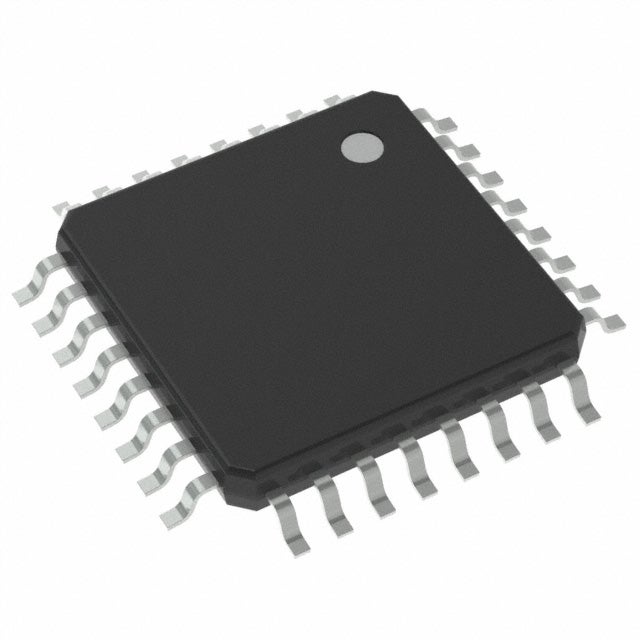
The ATmega328P is part of the ATmega328 product line. This product line contains multiple 8-bit microcontrollers of different shapes, sizes, and pin configurations, as shown below.
The ATmega328P component package options
As illustrated, the ATmega328P is available in different standard IC package sizes. Consequently, designers should be careful when choosing the proper microcontroller for their project, as size and shape have significant impact on the PCB layout options.
Memory Options
Memory on the ATmega328P is programmable. This functionality; although beneficial, introduces the capacity for software bugs with the potential to impact processor execution. For less experienced programmers or designers, this could make it difficult to distinguish between hardware and software bugs when testing a project.
The ATmega328P does not contain a C compiler, so programmers must choose their own. Some C compilers do not contain certain bit definitions in their header files. Without these bit definitions, C code for the registers and memory will not compile, even if the code is correct. Programmers should look in the documentation for their C compiler to determine whether these bit definitions are properly supported.
The size of the flash memory boot loader section is modifiable, and the ATmega328P allows code to be read from memory at the exact same time as new code is being written. Since the boot loader section can write to itself, it means it is possible for incorrect code to overwrite the ability for the chip to boot properly. Proper maintenance of this feature allows programmers to modify boot instructions dynamically, but this should only be done with a thorough understanding of how this parallel execution works. This read-while-write functionality is a form of parallel programming, even though it’s only on one chip.
Programming
The ATmega328P datasheet describes the component as capable of handling complex instructions within a single clock cycle. This is possible because the chip is optimized for maximum efficiency and minimum power usage. 131 unique instructions are possible within the chip’s registers, and combinations of those instructions allow for high variability and fast execution. The ATmega328P connects all its general purpose registers to its arithmetic logic unit (ALU), which allows instructions in two different registers to be executed at the same time. Using a reduced instruction set computer (RISC) architecture, the microcontroller can process instructions up to 10 times faster than other comparable microcontrollers.
Another advantage of the ATmega328P is that programmers can customize its functionality through targeted programming of its registers. The datasheet includes many code samples in assembly language. For programming ease, samples are also provided in C code. The chip’s memory and its execution registers are both programmable, and the ATmega328P includes 32KB of onboard flash memory. This memory can be reprogrammed through multiple interfaces on the chip, and the flash memory does not interfere with execution in the general purpose registers. Designers can rely on the flash memory to handle at least 10,000 write/erase cycles. Since the flash memory is so flexible, security is a foremost concern. The memory is divided into two sections: a boot loader and an application program section, which is shown in the block diagram below.
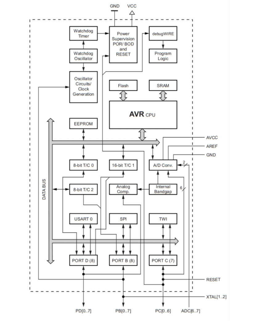
Block diagram of the ATmega328P microcontroller.
In addition to the considerations above, there are special considerations that are important to know that will impact the ATmega328p’s operation and performance.
Special ATmega328P Features
The ATmega328P has specialized features for power management: a brown-out mode and six different sleep modes. The brown-out detector (BOD) is not enabled by default, but when enabled, monitors the power consumption in sleep modes. Some sleep modes allow disabling of the BOD, which can save power, but this may also put other operations at risk if power is unexpectedly lost. While sleep mode is usually a simple idle, the sleep modes for the ATmega328P distinguish between idle, noise reduction, power down, power save, standby, and extended standby. Each of these states rely on different stimuli to know when the chip should wake up again.
All functions of the ATmega328P are optimized for speed, but depending on the type of programming or data writing being done, different operations are completed in different time periods. Assuming nothing impedes the writing operations, the ATmega328P can write or erase data within a time interval of 1.7 to 4.5 milliseconds. This range of time can either be helpful or a hindrance to programmers, depending on how they handle chip interrupts during the writing process. Programmers should not rely on all writes happening in the same amount of time. In addition, programmers should be aware of the many different potential interrupt sources in both the hardware and software of the ATmega328P. This gives fine-grained control over execution and writing, but can be difficult to master.
Optimizing Your ATmega328P Board Design
The ATmega328P is a popular choice for many applications. These include power regulation, motor control, industrial equipment control, and in switch mode power systems (SMPSs). The microcontroller is also commonly used in commercial products for digital and analog signal processing, displays and peripheral interfaces. For all of these applications, the best PCB design is attained by following guidelines; such as below.
AT328P PCB Design Guidelines
- Choose the best package size for your design
- Use accurate component CAD models from a reliable source
- Follow good PCB layout practices
- Utilize AT328P datasheet data and examples
- Make use of reference boards and evaluation kits, as shown below
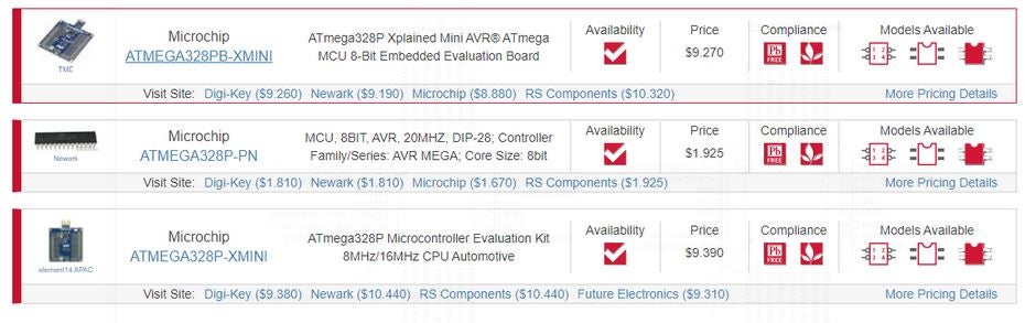 ATmega328P evaluation boards and kits from Ultra Librarian.
If you’re looking for CAD models for common components or important design aid for components like the AT328p microntroller, Ultra Librarian helps by compiling all your sourcing and CAD information in one place.
Working with Ultra Librarian sets up your team for success to ensure streamlined and error-free design, production, and sourcing. Register today for free.