
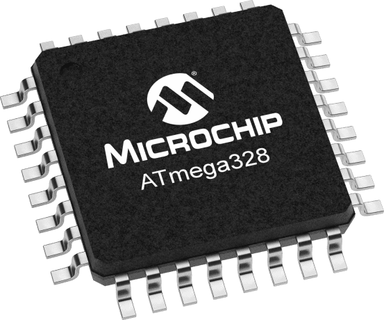
The ATmega328p microcontroller
The driver of smart electronics products and advanced electronics system technologies are the utilization of embedded systems. And the components that provide operational functionality and control are microprocessors (MPUs) and microcontrollers (MCUs). MPUs are typically highly integrated components used when extensive processing capability is required. MCUs are used for more specific functionality like industrial control or smart appliances.
Creating a quality circuit board design necessitates you institute best practices, such as following your CM’s DFM and DFA rules and guidelines to ensure your board can be built efficiently. The same is true for developing embedded systems; however, component selection, especially the MCU, is more important as it affects all aspects of your PCB layout. The ATmega328, by Microchip Technology Inc., is a good choice for many applications. However, to make the best package selection and fully leverage the advantages this MCU offers begins with understanding the AT328p328 pinout.
ATmega328p Uses and Applications
The ATmega328p is one of a series of 8-bit AVR MCUs built by Microchip that is relatively easy to implement for specific function devices and products. The chip has several features, including low power consumption and fast processing speed, that promote its use in many applications, as listed below.
Common AT328p Applications
- Industrial equipment control
- Motor control
- Power regulation
- Switch mode power systems
- Commercial product embedded systems
- Digital processing
- Analog signal acquisition and processing
- Peripheral interface
- Display devices
In addition to the applications listed above, the ATmega328p is probably most often used for development with Arduino boards; such as the popular UNO.
In the figure below, the block diagram of ATmega328p’s major operational units is shown.
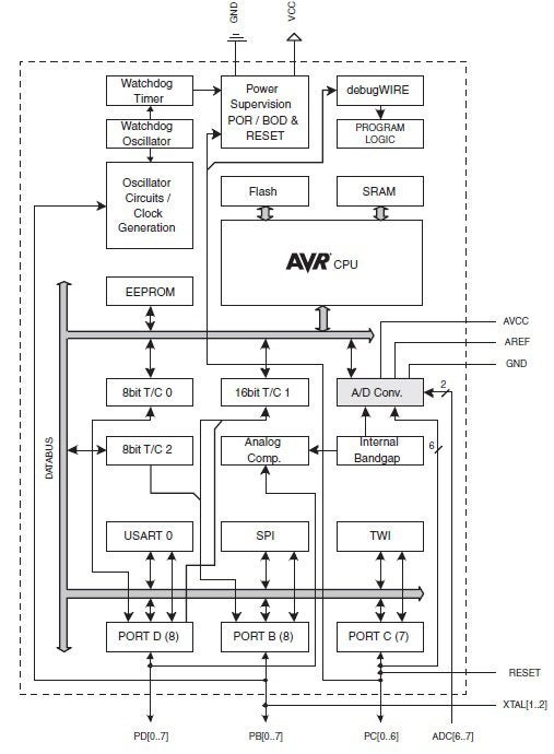
Block diagram of ATmega328p
Operationally, the MCU includes 32kb of programmable flash memory, 32 general purpose registers–of which two can be accessed during one clock cycle–, 2kb of SRAM, 1kb of EEPROM, and three timer/counters. To minimize power consumption and extend the component lifecycle, there are six power save modes: power-down, power-save, ADC noise reduction, standby, extended standby, and idle). The ATmega328 includes USART, SPI, and two-wire serial communication options distributed over 23 GPI/O lines. These and other external connections of the ATmega328p pinout are described below.
Understanding the ATmega328p Pinout
As discussed in the Atmega328p datasheet, the device is available in 28-pin SPDIP, 28-pin VQFN, 32-pin TQFP, and 32-pin VQFN. The ATmega328p pinout for each of these component packages is shown below.
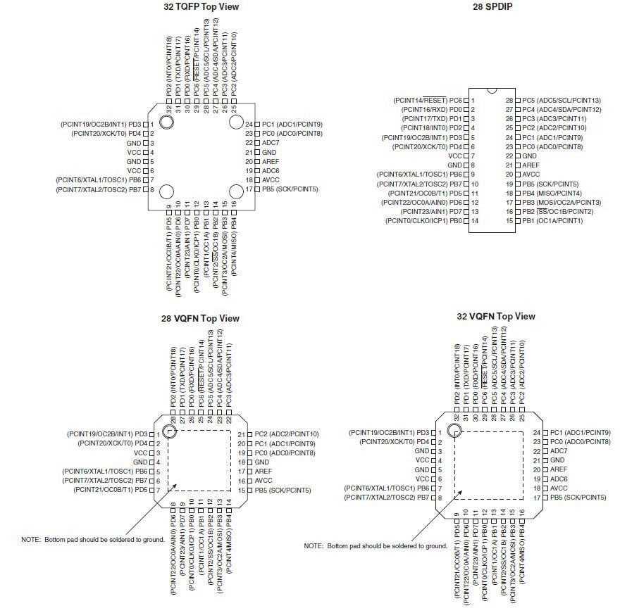
ATmega328p package pinouts
The pin descriptions for the pinouts are listed below.
As shown in the table, pin locations for the different MCU architectures vary. However, each device has 23 bi-directional I/O pins.
Please, see the ATmega328p datasheet for additional details concerning pin assignments and connections.
ATmega328p PCBA Design Optimization
When designing with the ATmega328p, you must select the best architecture or package type for your design, as errors could result in redesigns, respins, and additional development costs. These can be prevented by sourcing your schematic symbols, PCB layout footprints, and 3D CAD models from a reliable online component library, as shown below.
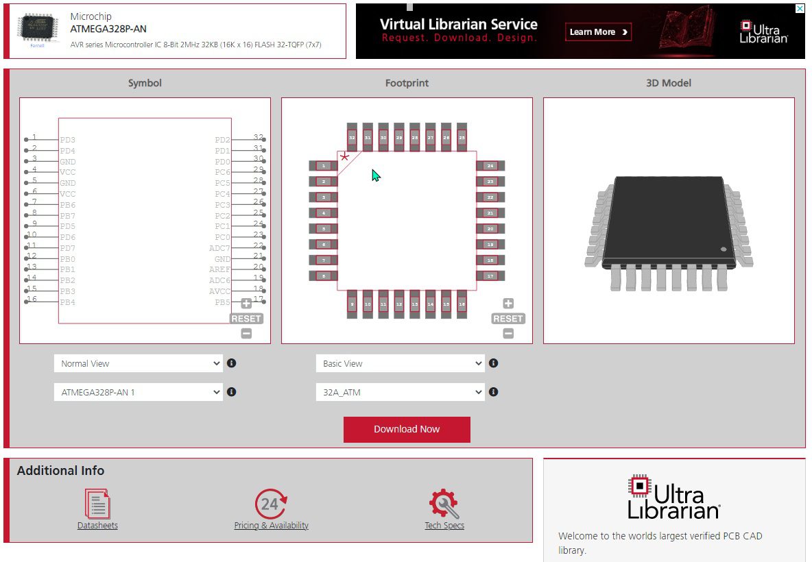
ATmega328p symbol, footprint, and 3D CAD model from UL
If you’re looking for CAD models for common components or design data like the ATmega328p pinout descriptions, Ultra Librarian helps by compiling all your sourcing and CAD information in one place.
Working with Ultra Librarian sets up your team for success to ensure streamlined and error-free design, production, and sourcing. Register today for free.


")
