
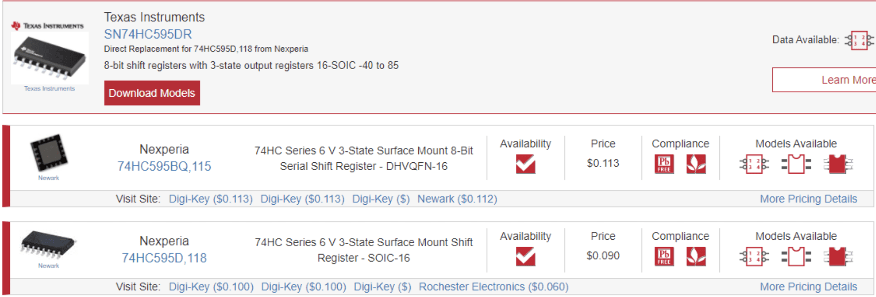
Shift registers move data within precise time intervals when making calculations in complex electronic components. The 74HC595 and its updated component, the SN74HC595, can both process and combine simple data into more complex calculations, driving calculators, computers, and other complex machines. These components and their variants can be used in serial or parallel circuits, with their own internal clocks, or with a component-wide clock.
An Overview of the 74HC595
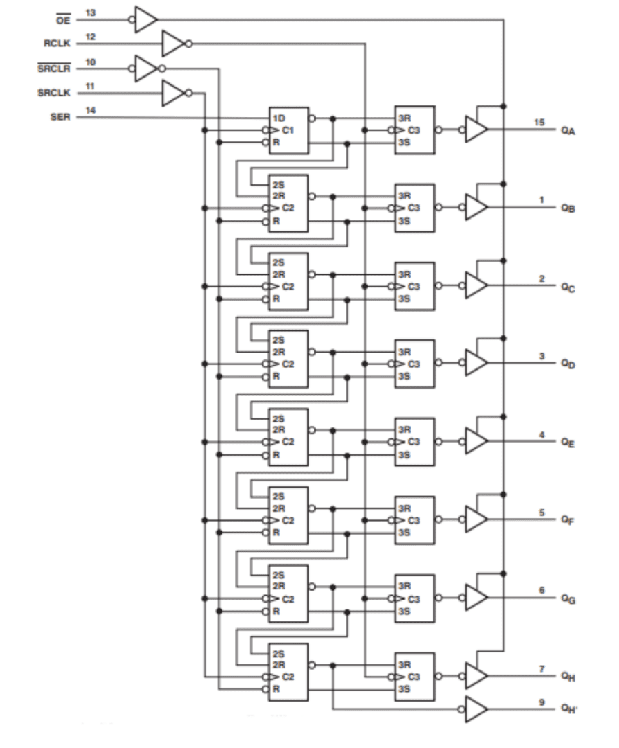
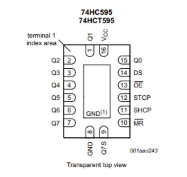
The 74HC595 is an 8-bit shift register that takes in serial input and can create either serial or parallel output. It has a variant component, the 74HCT595, which has a slightly different shape. Both components also contain a storage register and three separate outputs. The shift register and storage register each have their own clocks. If the clocks are connected together, the shift register clock will always be one cycle ahead of the storage register clock.
Input can be reset at any time by passing a low amount of current through a specific pin called the MR pin. Any data in the shift register is transferred to the storage register when a low level of current across another pin, the STCP pin, becomes a high level of current instead.
The 74HC595 operates in a voltage range of 2-6V, while the 74HCT595 operates within a narrower range of 4.5-5.5V. Although the 74HC595 can operate in a wider voltage range, it has a dramatically higher propagation delay than the 74HCT595. The 74HCT595 has a propagation delay just over a quarter of the 74HC595’s delay length—63 nanoseconds compared to 240 nanoseconds. This shorter delay means long delays are less likely to build up over time, which could cause an overall slowdown in an electronics project. A slowdown in a shift register, since its main function is to handle data, could be disastrous to computational speeds.
SN74HC595: The Updated 74HC595
The SN74HC595 operates in the same voltage range as its predecessor, and has a variant of its own, the SN54HC595. This updated component and its variant are not directly comparable to their predecessors in some ways, but have the same basic functionality. Both updated component variants operate in the same wide voltage range, and both updated components have a lower propagation delay than their predecessors, at only 13 nanoseconds. This reduced delay means these updated components process data much more quickly. The updated components consume 10mA more power than their predecessors, but this is a very small amount easily balanced by the increase in speed. The main difference between the two sets of components is the increase in speed; most other characteristics between the sets remain the same. This includes having 3 outputs, allowing conversion between single inputs and parallel outputs, and the existence of separate clocks for the storage and shift registers.
Uses for the 74HC595 and SN74HC595
By reading through their datasheets, it’s clear the primary purpose for the 74HC595 and SN74HC595, as shift registers, is data storage. They move binary data through their registers and can also perform simple calculations on that data. They are commonly used inside calculators for addition, subtraction, multiplication, and division, and simple operations can be combined quickly into more complex calculations. Computer systems have a similar mechanic for calculating data in registers, often connected to the CPU core clock in some way. Shift registers in calculators and computers can also calculate sequences of numbers and implement various types of counters. Since they can compute all four basic arithmetic operations, it doesn’t matter if a sequence is arithmetic or geometric.
Shift registers are also vital to converting input data into different forms for proper use. Serial input data can be converted into parallel output, while parallel input can be converted into serial output. It is much more common to convert data in this way, rather than to have parallel input and output or serial input and output. Serial input and output, in particular, is used to implement time delays, rather than take advantage of speed and computational power.
Ultra Librarian provides the 74HC595, its variants, and its updated component, allowing designers a variety of serial output shift registers to choose from. Working with Ultra Librarian takes the guesswork out of preparing your next great device and puts your ideas on the road to success. Register today for free.


")

