
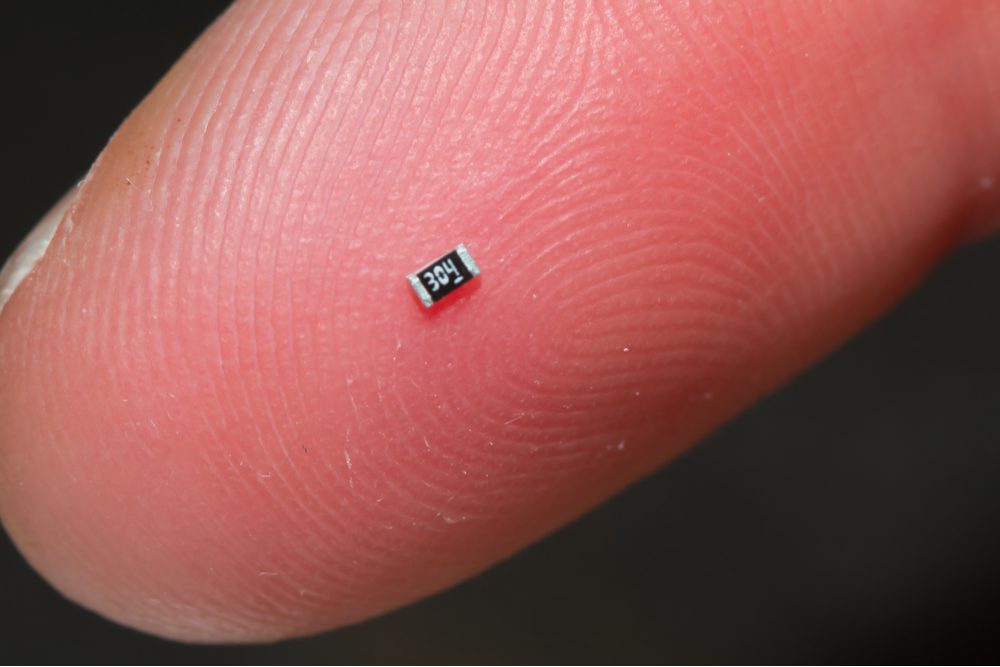
The shift from through-hole to surface-mount technology (SMT) transformed PCB design by enabling smaller, denser, and more efficient electronics. The 0603 package footprints offer an ideal balance between compact size, electrical performance, and manufacturability. They support high-density layouts while remaining suitable for automated assembly and manual prototyping.
This guide covers the essentials of 0603 components, including package dimensions, electrical characteristics, manufacturing considerations, and CAD footprint design.
0603 Imperial vs. 0603 Metric
One of the most dangerous traps in PCB design is the overlapping nomenclature between imperial and metric SMD sizing. When an engineer or datasheet refers to a “0603 component,” they are almost universally referring to the imperial version. However, failure to verify this can lead to disastrous manufacturing errors.
The naming convention relates to the length and width of the package.
- 0603 Imperial: 0.06 inches long by 0.03 inches wide. (This converts to 1.6 mm x 0.8 mm, which is known as the 1608 Metric code).
- 0603 Metric: 0.6 mm long by 0.3 mm wide. (This converts to 0.02 x 0.01 inches, which is the ultra-tiny 0201 Imperial package).
The Golden Rule: Always assume “0603” means the imperial (1.6 mm x 0.8 mm) package unless you are reading a specifically metric-first datasheet. To avoid layout failures, always double-check the “Package Outline Dimensions” chart in your manufacturer’s datasheet before drawing your 0603 package footprints.
0603 Package Footprints Standard Dimensions
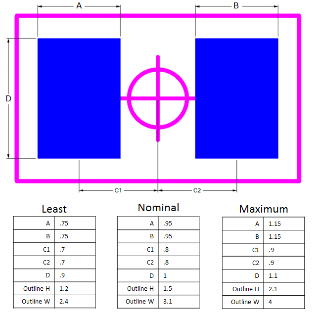
Because the IPC-7351 standard provides specific guidelines for land patterns based on assembly density, not all 0603 pads are exactly the same size. The physical package has standard dimensions, but the copper pads (the footprint) must be slightly larger to accommodate the solder fillet.
When designing pads for 0603 components, engineers may also consider the component type and manufacturing requirements. A 0603 resistor and a 0603 capacitor share the same nominal package dimensions. However, factors such as terminal geometry, assembly process, soldering method, component tolerances, inspection requirements, and reliability goals can influence the final pad dimensions. High-reliability, hand-soldered, or rework-prone designs often use larger pads, while high-density assemblies may use smaller land patterns to conserve board space.
Standard Physical Dimensions (Imperial 0603 / Metric 1608)
| Dimension | Typical Value (mm) | Typical Value (in) | Tolerance (mm) | Tolerance (in) |
| Length (L) | 1.60 | 0.063 | ± 0.10 | ± 0.004 |
| Width (W) | 0.80 | 0.031 | ± 0.10 | ± 0.004 |
| Height (H) | 0.45 (varies by part) | 0.018 (varies by part) | ± 0.10 | ± 0.004 |
| Terminal (T) | 0.30 | 0.012 | ± 0.20 | ± 0.008 |
IPC-7351 Land Pattern Density Levels
When designing 0603 package footprints, you should select a density level that matches your manufacturing goals:
- Density Level A (Maximum): Features the largest pads. Ideal for low-density boards, wave soldering, or components subjected to high vibration/shock where maximum solder joint strength is required.
- Density Level B (Nominal): The industry standard. Provides a balance between a solder fillet and efficient use of PCB real estate. Most pre-built libraries use this standard.
- Density Level C (Least): Uses the smallest possible pads. Reserved for ultra-high-density boards (like mobile phones) where space is at a premium.
Electrical Ratings for 0603 Passive Components
While the footprint geometry is standardized, the electrical capabilities of 0603 components vary widely depending on the material chemistry (e.g., thick-film vs. thin-film resistors, or X7R vs. C0G dielectrics for capacitors). Here are typical and high-performance limits you will encounter when sourcing 0603 passives.
0603 Passive Components Ratings
| Parameter | Standard Typical Value | High-Performance Value |
| 0603 Resistor Ratings | ||
| Power Dissipation | 1/10 W (0.1 W) | Up to 1/4 W (0.25 W) for high-power thick-film |
| Max Working Voltage | 50 V | 75 V to 100 V (Anti-surge models) |
| Resistance Range | 1 Ω to 10 MΩ | Milli-ohm (current sense) to Giga-ohm ranges |
| Tolerance | 1% or 5% | As tight as 0.01% (Precision thin-film) |
| 0603 Capacitor Ratings (MLCCs) | ||
| Capacitance Range | 1 pF to 1 µF | Up to 10 µF or 22 µF (Requires careful DC bias consideration) |
| Voltage Rating | 10 V, 16 V, 25 V | Up to 250 V (usually limits max capacitance to < 10 nF) |
| Dielectrics | X7R, X5R | C0G/NP0 (Ultra-stable, but low capacitance limits) |
| 0603 Inductor Ratings | ||
| Inductance Range | 1 nH to 470 nH | 1 µH to 22 µH |
| Current Rating (I_dc) | 50 mA to 300 mA | Up to 1.5 A – 2.0 A |
| DC Resistance (DCR) | Very low (milli-ohms) | Higher (can reach several ohms at high inductance) |
Note: For Multi-Layer Ceramic Capacitors (MLCCs), high capacitance in a small package results in a severe “DC Bias Effect,” meaning the effective capacitance drops significantly as the applied voltage increases.
Manufacturing and Assembly Considerations
The 0603 package is generally highly manufacturable, but specific guidelines must be followed to ensure high yields.
- Pick-and-Place: 0603 components are heavy and large enough that standard vacuum nozzles on SMT pick-and-place machines consistently achieve high placement accuracy, though exact rates depend on equipment calibration, nozzle condition, and process control. They do not suffer from the extreme static-cling issues that plague 0201 or 01005 packages.
- Tombstoning Prevention: Tombstoning occurs when solder paste on one pad melts before the other, pulling the component vertically. To prevent this, ensure your 0603 package footprints have perfectly symmetrical pads. Additionally, if one pad connects to a massive ground plane, use thermal relief spokes to ensure both pads heat up at the same rate during reflow soldering.
- Soldering Methods: 0603 components are optimized for reflow soldering. However, unlike smaller packages, 0603s can be wave-soldered if they are glued to the bottom of the board prior to passing over the solder wave.
How to Import 0603 Package Footprints from Ultra Librarian in Major ECAD Tools
Rather than risking manual drafting errors, engineers rely on verified CAD libraries to source accurate 0603 package footprints. When you download a verified 0603 model from Ultra Librarian, integrating it into your software is smooth.
The general process for any ECAD tool involves downloading the footprint files, placing them in your library directory, and pointing your software to that path. When using Ultra Librarian, the steps for each major platform are as follows:
- Altium Designer: Ultra Librarian provides a direct .lia script or an integrated Altium plugin. Simply run the script to automatically generate the schematic symbol and the 0603 footprint, and attach the 3D STEP model directly into your component library.
- Cadence OrCAD X/Allegro X: Downloads include a batch file (.bat). Running this creates the necessary .pad and .dra files. Ensure your padpath and psmpath in Allegro’s User Preferences are pointing to the folder where you saved the files so the software can locate the footprint.
- KiCad: Ultra Librarian exports native .kicad_sym and .kicad_mod files. Simply move the footprint file into your designated .pretty folder, map the 3D .step file within the footprint properties, and it is ready for layout.
Source Verified Models with Ultra Librarian
Designing a reliable PCB requires absolute confidence in your component data. Pulling 0603 package footprints from unverified forums or drafting them from a datasheet introduces unnecessary manufacturing risk.
Ultra Librarian helps by compiling all your sourcing and CAD information in one place. We provide access to manufacturer-verified, IPC-compliant schematic symbols, PCB footprints, and 3D models for millions of components, including a vast array of 0603 package footprints. By downloading native files for your specific ECAD application, you eliminate footprint mismatch errors and ensure your design is ready for production.
Working with Ultra Librarian sets your team up for success, ensuring streamlined and error-free design, production, and sourcing. Register today for free.

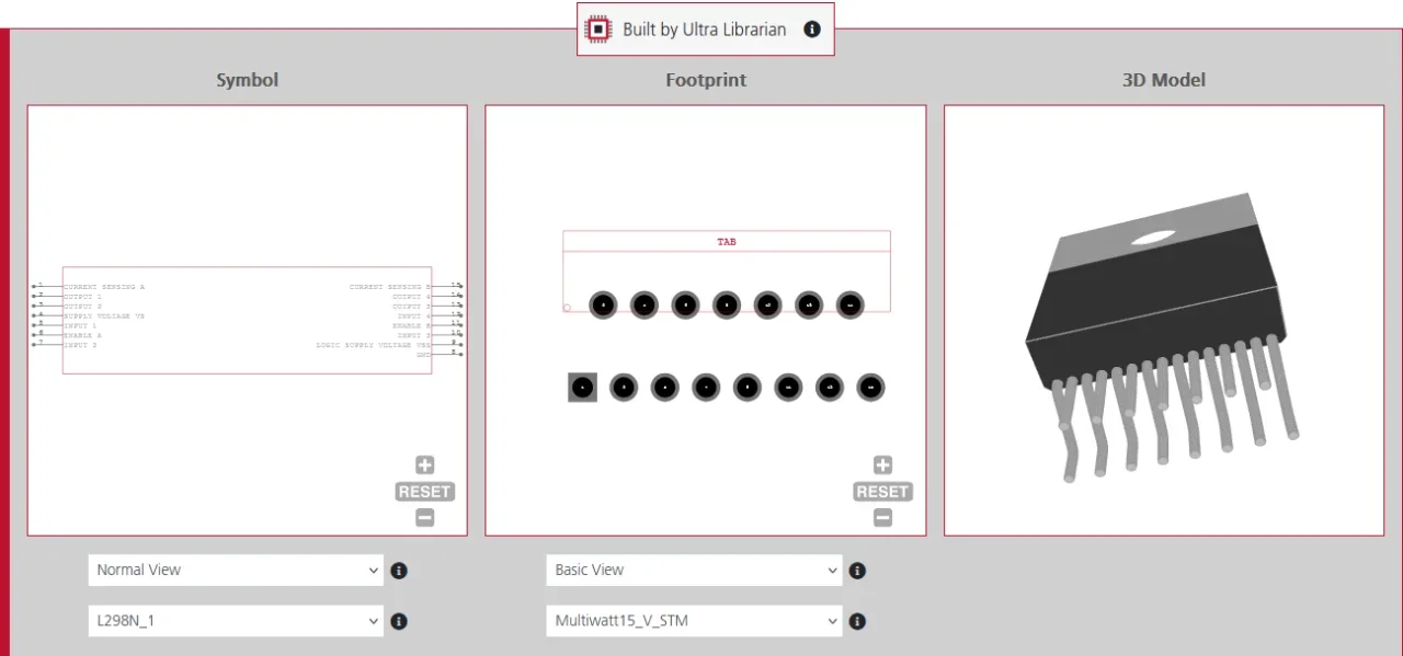
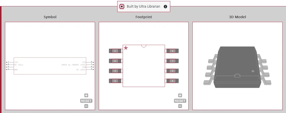
 If you’re looking for any of our component footprints or models, we have readily available and free options for you and your design team. Search our library for the solution you’ve been looking for.