Nowadays, we use memory, microcontrollers, and many complex integrated devices in our system. Sometimes, they may face one or more problems such as over-temperature, processor lockup, or safety lock failure that require external intervention. Under such a situation, even a single error flag is sufficient to trigger a system management IC to take swift action without knowing which device or module has the error.
In this regard, a quadruple 2-Input OR gate, like SN74HC32N, can use fewer inputs to monitor error signals, thus increasing the operation frequency. Before we look at some of the essential elements of the device from the SN74HC32N datasheet, let’s have some essential knowledge supplements.
OR Gate Fundamental
An OR gate gives a high output when at least one of the inputs is high. The basic boolean expression is as follows:
Y (output) = A+B (logical sum of inputs)
The truth table is as follows.
| Y | A | B |
| 0 | 0 | 0 |
| 0 | 1 | 1 |
| 1 | 0 | 1 |
| 1 | 1 | 1 |
The above truth table shows that if any of the two inputs detect an error (high), the output will show an error (high). We can use a 2-input OR gate to combine error signals from two different sources to trigger a protecting device. Likewise, we can use two or more OR gates in parallel to combine error signals from multiple sources into one output. This is the fundamental of the SN74HC32N device.
Analyzing the SN74HC32N Datasheet
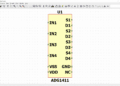
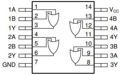
The device contains four independent 2-input OR gates. The functional pinout diagram is as follows.
Maximum Ratings and Characteristics
The absolute maximum ratings of the SN74HC32N are as follows:
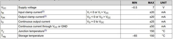
Operating the device beyond the Absolute Maximum Rating over an extended period of time may affect its reliability. The device may be subjected to overcurrent beyond the max rating by adding a series resistor at the output, but the electrical and thermal limits should be followed at all times.
The maximum value of this external resistance is calculated by dividing the max input voltage by the max input leakage current as mentioned in the SN74HC32N datasheet.
Functional Diagram
The functional diagram of SN74HC32N IC has been shown below.
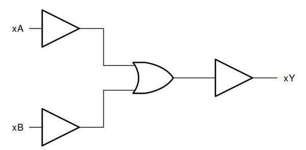
The functional table of this logic gate is as follows.
| Inputs | Output | |
| A | B | Y |
| Low | Low | Low |
| High | Low | High |
| Low | High | High |
| High | High | High |
As you can see, if any one of the inputs is high, the output will be high. In simple terms, if anyone or more of the OR inputs detect an error signal, the output will result as an error signal.
SN74HC32N Features
Balanced CMOS Push-Pull Output
As it features a balanced topology, you get an optimized and balanced output drive. Thus, it allows the device to source and sink similar currents. However, it is still possible to handle large loads without damaging the device due to over current provided the Absolute Maximum ratings are in check, as mentioned in the SN74HC32N datasheet.
It is possible to configure SN74HC32 to drive large capacitive loads beyond recommendations, provided you can lower the output current to maximum ratings through an output resistor.
Combine Error Flags
Let’s consider a situation where a fan driver module will activate if any of the four devices get overheated. In this regard, we can use OR gates to combine error signals into one output.
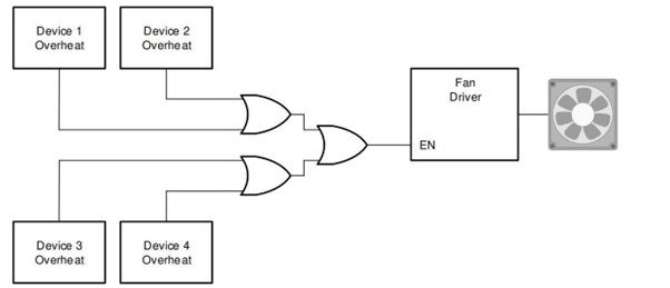
The above diagram shows three 2-input OR gates receiving signals from four independent devices to operate a fan module in case of an overheating situation. If any one of the devices gets overheated, the output of the three 2-input OR gates will be positive. Here, we can use three 2-input OR gates of the SN74HC32N IC to combine error signals from four different systems into one. The fourth OR gate can be grounded or can be used for any other application.
Package and Design
The SN74HC32N comes in various packages; SOIC, SSOP, PDIP, SO, TSSOP, CDIP, CFP, and LCCC. All are 14-pin packages except for LCCC, which is a 20-pin configuration. More details regarding the packages are available in the SN74HC32N datasheet.
One of the important considerations while using such a multi-input device is that the unused input should always be grounded. If the unused inputs are left in a floating state, the device will experience undefined voltages at the outside connections, leading to undefined operational states.
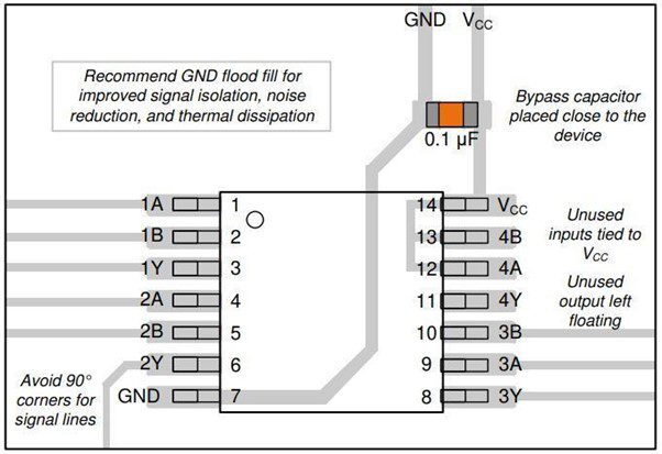
It is imperative to add a decoupling capacitor between the source and the ground, as shown in the figure below.
To ensure optimal device performance, the maximum output capacitive load should not exceed 70 pF. Similarly, the resistive load at the output should be designed to ensure the device output current does not exceed the Absolute Maximum Rating. Additionally, to overcome noise interference, you can use one or more bypass capacitors (0.1-μF) at the Vcc terminal in parallel.
Apart from the data provided in the SN74HC32N datasheet, you will need ECAD/MCAD models along with reliable sourcing information to aid your design process. The parts search feature in Ultra Librarian will help you access all those essential information with ease. All ECAD data you’ll find on Ultra Librarian is compatible with popular ECAD applications and is verified by component manufacturers to help streamline your designing process.
Working with Ultra Librarian sets up your team for success to ensure streamlined and error-free design, production, and sourcing. Register today for free.