
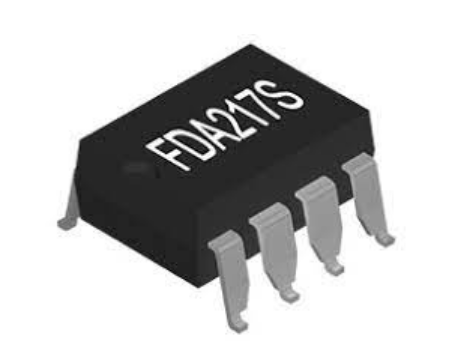
FDA217 Photovoltaic Driver
Metal-Oxide Field Effect Transistors (MOSFETs) are among the most versatile and implemented active electronic components. These semiconductors are often preferred for switching applications as compared to diodes or other transistors. However, drivers are typically needed to leverage the advantages of these fast transition devices.
A commonly utilized MOSFET driver for high-power applications is the IXYS FDA217 available from TME Electronic Components. This device employs photovoltaics to achieve good galvanic isolation, which is a requirement in the presence of transients and noise that can affect MOSFET performance. For the best PCB design, the important information and data; such as features, applications, and specifications, from the FDA217 datasheet should be leveraged.
FDA217: Features and Applications
The FDA217 is a feature-rich optical MOSFET driver versatile enough to be used in various switching and process control applications as listed below.
As shown above, the FDA217 can be employed in multiple electronic configurations where isolation is a primary design directive. The component also has negligible EMI/RFI generation which makes it especially suitable for transient environment application.
FDA217: Parameters and Specifications
According to the FDA217 datasheet, the device has the following maximum electrical and thermal ratings.
1 Derate linearly 1.33mW/°C
2 Derate output power linearly 6.67mW/°C
An important attribute of the FDA217 is the ability to discharge gate current from internal circuitry when LED excitation current is removed. This feature avoids the space and cost requirements of external circuitry, which can be important design considerations for opting for this MOSFET driver. Below are the electrical specifications for the FDA217.
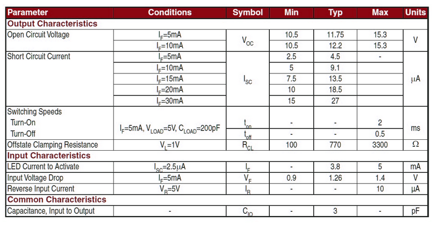
FDA217 electrical specifications
The above functionality enables the FDA217 to achieve 3750 Vrms isolation between input and output.
FDA217: Layout and Operation
The component pinout and functional diagram, also provided in the FDA217 datasheet, is shown below.
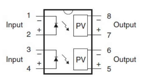
FDA217 pinout
Two of the most important operational parameters for switching devices like the FDA217 are Turn-On and Turn-Off time, which are illustrated below versus load capacitance.
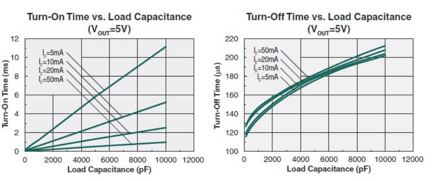 FDA217 transition times vs load capacitance
As shown, Turn-On transition time varies with current over the load capacitance range. However, Turn-Off time is relatively constant irrespective of current. Similarly, Turn-On transition varies and Turn-Off transition is more consistent versus temperature for various current levels.
PCB Design with the FDA217 Datasheet
The datasheet also includes important component data for the PCB layout. As shown below, the FDA217 is available as a surface mount and through-hole part.
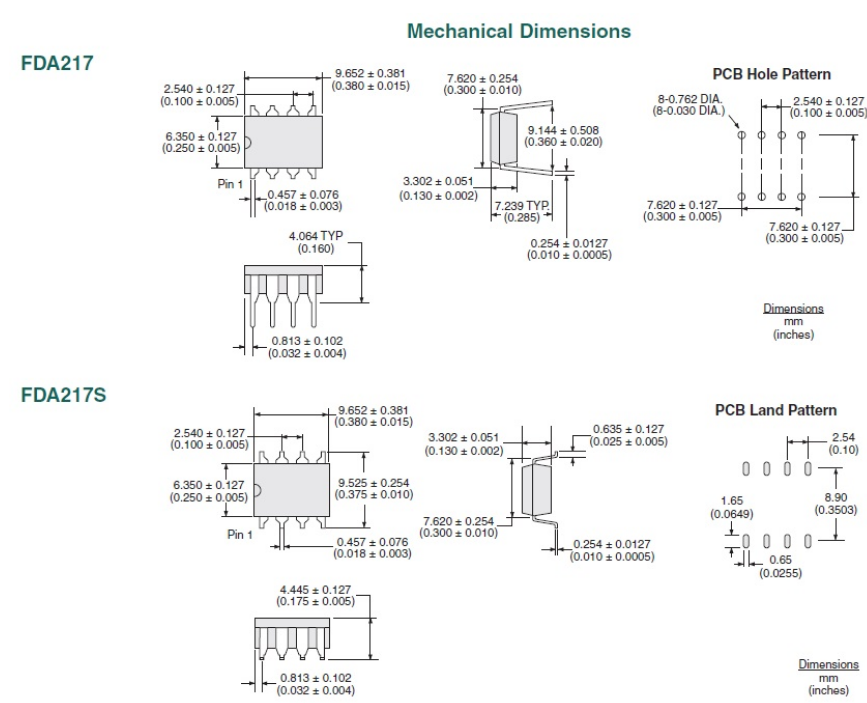
Through-hole and surface mount dimensions for the FDA217
Although, this information is helpful it is not advisable to create PCB footprints manually. The room for error is relatively high and the redesigns, turnaround time delays and additional costs that you may incur can be significant.
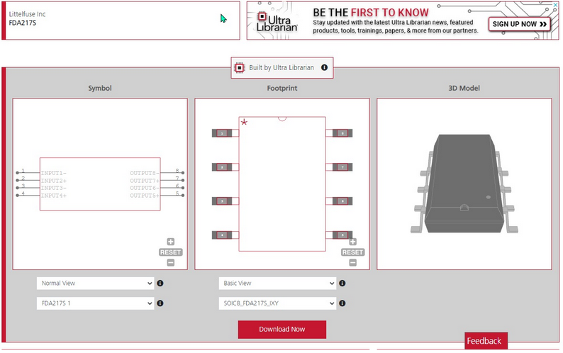
FDA217 schematic symbol, footprint and 3D CAD model from UL
A more reliable alternative is to source schematic symbols, footprints and 3D CAD format models from a trusted resource, as shown above, and procure the FDA217 from a reliable distributor.
If you’re looking for CAD models for common components or important design information like how to best use the FDA217 datasheet for your PCB project, Ultra Librarian helps by compiling all your sourcing and CAD information in one place.
Working with Ultra Librarian sets up your team for success to ensure streamlined and error-free design, production, and sourcing. Register today for free.


")

