Augmented reality software like InspectAR can play a useful role in PCB debugging
Let’s set the scene: you’ve just received a batch of boards from fabrication and you’re starting board-level tests. Working through testing in a complex layout requires careful checks of all aspects of the design, including measurements on component pads, connector pins, and exposed copper to verify connectivity. Normally, the designer or test engineer needs to have their PCB layout on a screen next to the board to ensure they can navigate the design, verify tests are passed, and ensure the correct points are being probed in the layout.
While augmented reality seems to have become another tech buzzword, it is making its way out of the lab and into practical applications and products. One important area where augmented reality tools can play a role is in test and debug, particularly for complex multi-layer PCBs with multiple connectors, dense components, and bus protocols with multiple branches. New software tools—like InspectAR—are enabling new methodologies that can help streamline PCB debugging, testing, and board bring-up during development, testing, and manual assembly. By superimposing your layout data on top of your PCBA, InspectAR gives designers a new perspective on their boards that can help speed up important design evaluation tasks.
The Look and Feel of Augmented Reality in PCB Debugging
Augmented reality tools like InspectAR provide a simple but important function: they allow design data from your PCB layout to be overlaid on top of your real circuit board. This can be done in real-time as you inspect and debug your board using your phone, webcam, or computer screen.
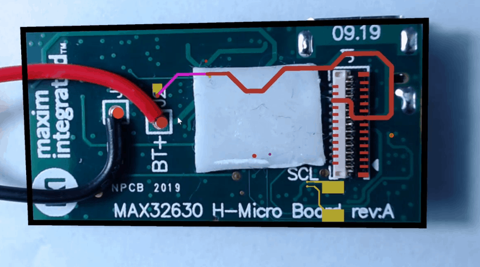
Net information overlaid between J2 and a pin on connector J1
With net information overlaid directly on top of your circuit board, it is easy to spot exactly which connections should be tested. PCB debugging tasks are much easier when you can see an overlay of your PCB layout data on top of your physical board. During testing, you can quickly compare basic test results with expected electrical behavior and you can quickly pinpoint defects in exact locations in the PCB layout.
Spotting Defects
When you can see the design overlaid on your circuit board, it is very easy to spot opens and shorts throughout the design, verify connectivity around the design, and see where components are connected without manually scanning through your layout. Measurements can be easily compared with your layout to verify connectivity, and you can spot other areas in the design to narrow down where a potential connectivity break might have occurred.
A connectivity problem can result in rework or a scrapped board, but overlaying the design data on the PCB layout helps designers distinguish when a board should be scrapped or when it is eligible for rework. It can also help distinguish design mistakes from quality defects, which will help you plan to correct problems and prevent other defects in the future. InspectAR can be used to more easily identify defects in a design, including:
- Shorts or opens due to defects: Sometimes, a short or open is not due to a mistake in the design. Instead, it may be a fabrication defect. Overlaid connections in the design data vs. real connections on the board allow an immediate comparison, and it helps the specific defect to be diagnosed without more expensive inspection equipment.
- Incorrect footprints: It is always possible a component has a slight PCB footprint mismatch and the assembler doesn’t notice. This tends to happen when the footprint is slightly larger than the pad arrangement, leading to incorrect electrical behavior and measurements.
- Misplaced or unnecessary components: Sometimes, you may find components are misplaced or unnecessary, and this may cause problems found during testing or board bring-up. Some great examples are address-select connections, jumpers, or resistors on SOP pins.
- Tombstoned components: Some tombstones are very obvious, but others can be imperceptible without a microscope or without carefully probing multiple points along a circuit. Having the layout overlaid on your board helps you spot when a component might be tombstoned or defective.
These are some of the most common problems that might result in a scrapped or reworked board, but the possibilities are endless. If you’ve narrowed down your defects to a component problem, an augmented reality software like InspectAR can give you access to datasheets by pulling MPNs from your BOM and schematics. Again, you can compare component data with your measurement results to determine if a fab/assembly defect is causing a problem or if an alternative component is needed.
How InspectAR Aids PCB Debugging
InspectAR is one of the newest augmented reality tools specialized for PCB design, testing, debugging, and inspection. By visually comparing an assembled board with an overlaid view of the PCB layout, InspectAR can help users diagnose the above defects as they work through testing and inspection tasks. Inspect AR uses your computer’s webcam or your phone’s camera to capture an image of your circuit board, and the PCB layout data will be overlaid on top of the design.
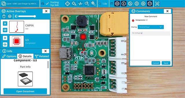
While working through testing tasks, a component can be selected in the circuit board image on the screen, and this will activate an overlay that displays the board layout data on top of the circuit board image. All component data is pulled directly from Digikey and displays alongside the PCB layout data on your screen. There is no need to flip back-and-forth between your design and your physical board—everything is present in a single streamlined interface.
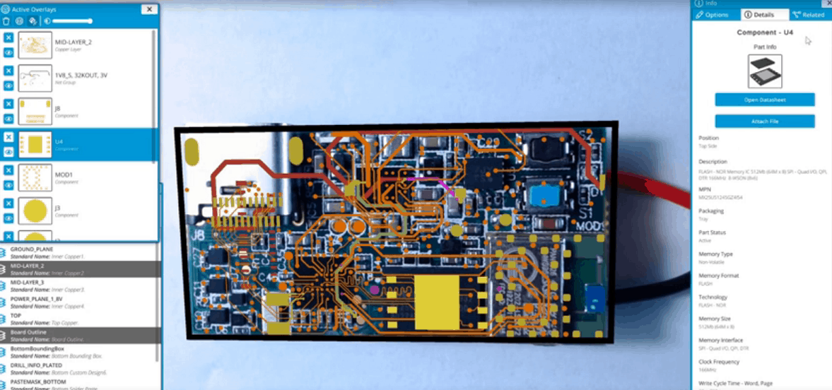
InspectAR users can see their PCB layout data and component information overlaid on their PCBA as they work
Since accurate CAD data is so important for comparing real boards with design data, make sure you use the best electronic parts search engine to find verified PCB footprints, symbols, and 3D STEP models. When you need to find ECAD models that are verified by component manufacturers, try using the electronics search engine features in Ultra Librarian. Once you’ve built and assembled your board, use the augmented reality features in InspectAR for PCB debugging. Both platforms are compatible with popular ECAD applications and will help you streamline your verification process.
Working with Ultra Librarian sets up your team for success to ensure streamlined and error-free design, production, and sourcing. Register today for free.