Creativity is undoubtedly one of the greatest attributes of a good PCB designer. However, it is not necessary to begin every design from scratch. Often, it is more efficient and cost-effective to rely on a previously vetted reference design, like an evaluation or development board. A good example is the small form factor board described by the RP2040 Zero datasheet.
RP2040 Zero Datasheet Design Information
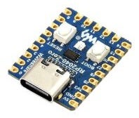
The RP2040 Zero (from the RP2040 datasheet, at left) is a small-form-factor reference board developed by Waveshare. Its compact size, low cost, and ease of implementation make it a favorite for PCB designers at all levels of expertise, but especially for DIYers, students, and early career engineers. The PCB is also available with presoldered pins for placement as a subdesign.
As shown in the RP2040 Zero datasheet, this development board, built to leverage the capabilities of the Raspberry Pi RP2040, has the following features:
RP2040 Zero Features
|
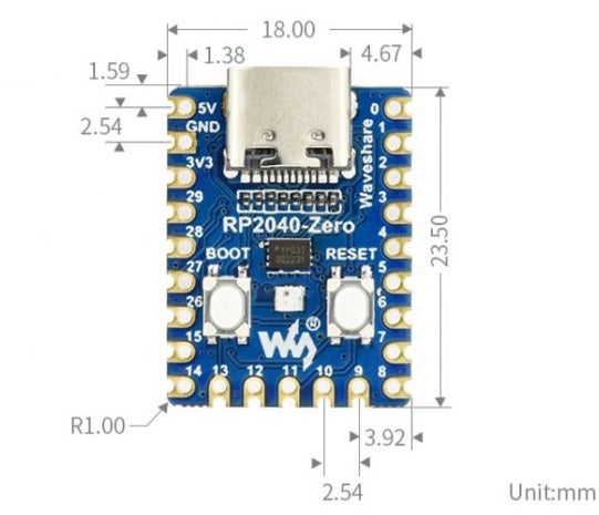
The board layout is shown below.
RP2040 Zero Pinout
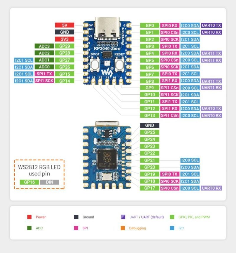
As shown above, the bopard is equipped with several communication options. These include Universal Asynchronous Receiver/Transmitter (UART), Inter-Integrated Circuit (I2C), and Serial-Peripheral Interface (SPI)connecto, as well as multiple General Purpose Input/Output (GPIO) pins that can be configured as needed.
The RP2040 Zero is one of many reference designs built around Raspberry Pi’s 2040 microcontroller. Alternatives include the Raspberry Pi Pico, Pico H, and Pico W; Arduino’s Nano RP2040 Connect; Sparkfun’s Pro Micro RP2040 and Thing Plus RP2040; Adafruit’s ItsyBitsy, Feather, and QT PY; and others. This popular MCU has many features that make it attractive, especially for compact applications.
RP2040 Microcontroller: Features and Operation
The RP2040 is a popular microcontroller due to its high-performance and flexibility for digital circuit implementation. Key features include:
RP2040 Features
|
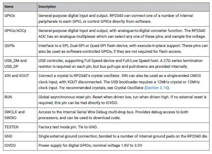
RP2040: Pinout and Descriptions
The pinout for the RP2040 is shown below.
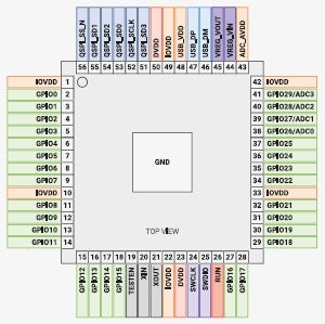
As shown above, and described below, the 56-pin IC is dominated by 30+ GPIO pins and multiple communication options.
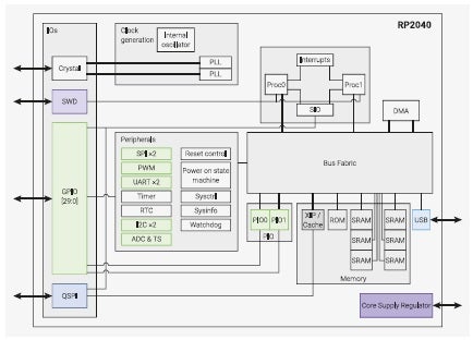
RP2040: Architecture and Operation
The RP2040 can safely operate at power levels between 1.8 and 3V DC. Additionally, it includes thermal management in the ADC circuitry. The large GPIO bank offers a great deal of flexibility with most pins configurable as I2C, UART, PWM, and SPI. Please see the RP2040 datasheet for detailed instructions for programming the microcontroller and interface configurations. The internal operational layout diagram is shown below.
Optimizing Your RP2040 Zero PCB Design Workflow
Designing applications with reference designs can be a tremendous advantage in terms of development time and cost. However, it is important to only rely on accurate and verified design data and information; including schematic and package diagrams and dimensions, respectively. For the RP2040 Zero, these are shown below.
RP2040 Zero Datasheet Essentials
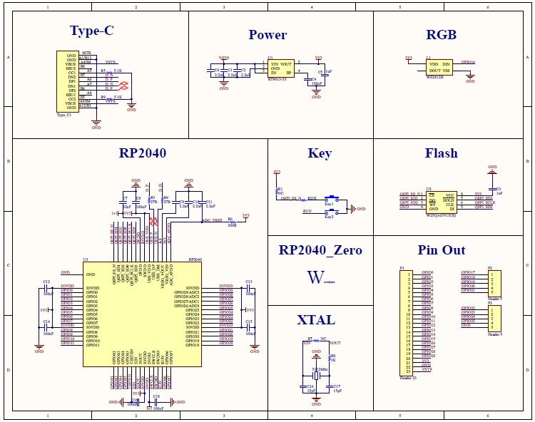
The most critical design decision when using reference designs is to ensure the board focus device meets your requirements. In addition to datasheet specifications, it is often necessary to model the primary component for component or circuit simulations/testing. In these cases, it is important to ensure your CAD models, as shown below, are accurate, satisfy industry standards, and are manufacturer-vetted.
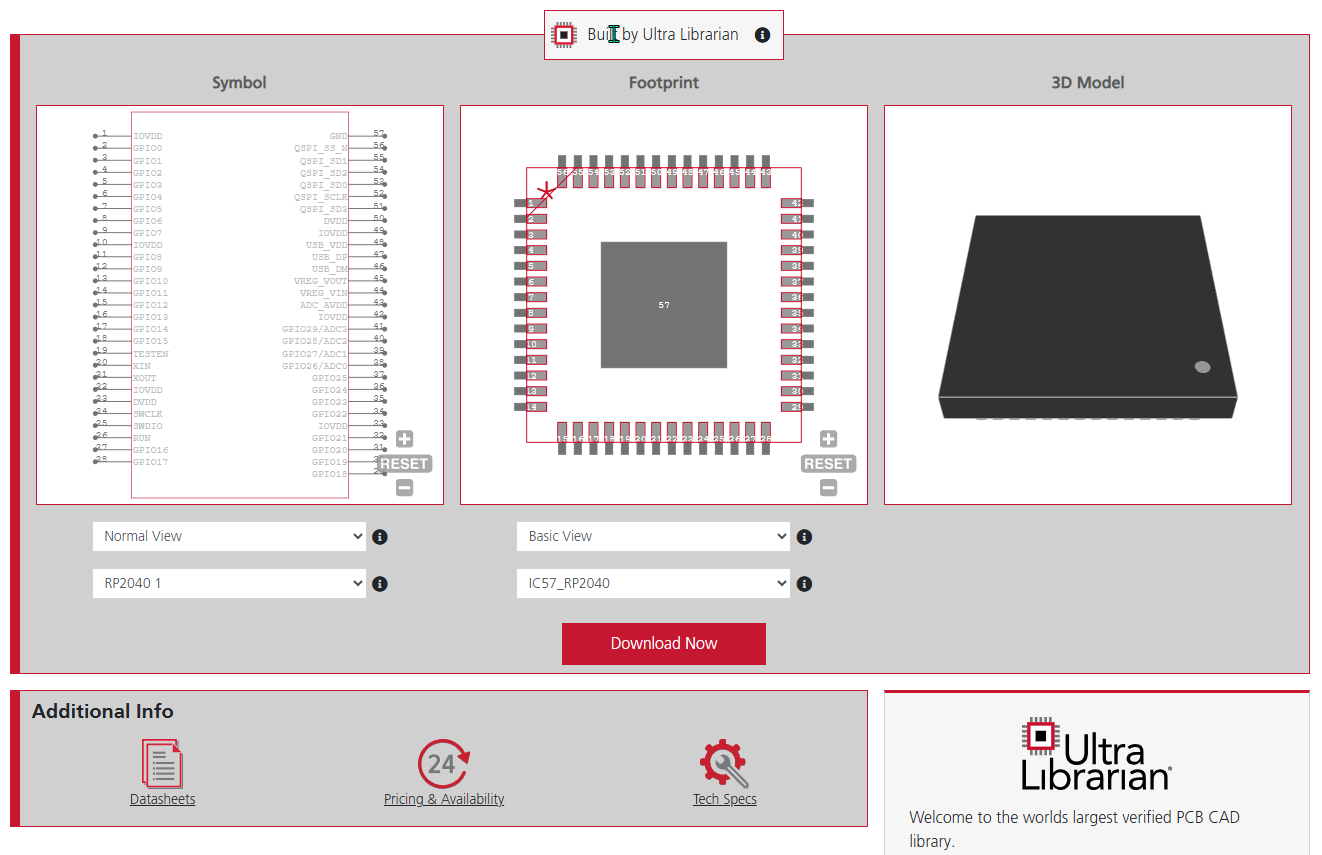
If you’re looking for CAD models for common components or important information like RP2040 Zero datasheet & pinout design specifications and analysis, Ultra Librarian helps by compiling all your sourcing and CAD information in one place.
Working with Ultra Librarian sets up your team for success to ensure streamlined and error-free design, production, and sourcing. Register today for free.