Representations of the ULN2803CDWR Darlington transistor array (Source: DigiKey)
The ULN2803CDWR is a versatile driver integrated circuit that bridges the gap between low-voltage logic and high-power loads such as motors or banks of bright LEDs. The ULN2803CDWR is a new version of the now-obsolete ULN2803ADWR, an 8-channel Darlington transistor array designed to take logic-level inputs, typically from microcontrollers, chips, or logic gates, and drive much higher current and voltage outputs.
Each of the eight channels can sink up to 500 mA and handle voltages of up to 50 V, making the ULN2803CDWR ideal for directly controlling relays, solenoids, stepper motors, and LED displays. This article serves as a quick reference guide to the ULN2803CDWR datasheet and the ULN2803ADWR datasheet (now obsolete), highlighting its key features, package options, and practical implementation details for design engineers.
ULN2803CDWR Datasheet: Features and Applications
At their core, the ULN2803CDWR and the ULN2803ADWR consist of eight NPN Darlington pairs. A Darlington pair, an invention by Sidney Darlington, connects two bipolar transistors such that the current amplified by the first is further amplified by the second. This configuration results in a high current gain, allowing a small input current from a logic signal to control a significantly larger output current. The ULN2803CDWR and ULN2803ADWR are designed for switching inductive loads and include internal freewheeling diodes, which provide a path for current when the load is switched off, preventing voltage spikes that could damage the circuit.
ULN2803CDWR Key Features
In looking at the ULN2803CDWR datasheet, you’ll see that it consists of a Darlington transistor array designed to interface low-power logic circuits with high-current or high-voltage loads.
- Eight Darlington Transistor Arrays – Includes eight independent NPN Darlington pairs in a single package, allowing control of up to eight separate loads simultaneously while saving PCB space and reducing component count.
- 500 mA Rated Collector Current – Each output can sink up to 500 mA of continuous current, allowing for the direct drive of high-current loads, such as relays, solenoids, and small motors, without the need for additional driver stages.
- High-Voltage Outputs (Up to 50 V) – Capable of handling output voltages up to 50 V, for uses in higher-voltage systems like 12 V or 24 V automotive or industrial applications.
- Internal Freewheeling Diodes – Built-in common-cathode clamp diodes protect the transistors from the high-voltage “kickback” generated by inductive loads when switched off.
- Logic-Level Compatible Inputs – Designed for direct interfacing with TTL and 5 V CMOS logic signals, simplifying the connection between low-power microcontrollers or logic circuits and high-power loads.
Common applications of the ULN2803CDWR include driving relays, solenoids, lamps, small stepper motors, and LED or gas-discharge displays, where the inductive nature of the loads can generate voltage spikes and require significant current sinking. For systems that require currents greater than 500 mA, multiple Darlington channels can be connected in parallel to increase the total current sinking capability.
ULN2803ADWR ReplacementIf you’re looking for a ULN2803ADWR replacement, the ULN2803CDWR is an updated part that retains the same core electrical specifications and pin layout, but adds two no-connect pins at the bottom of the package (pins 10 and 11). Key improvements include a higher thermal rating and an active product status compared to the older, phased-out ADWR. However, it is not a drop-in replacement due to the additional pins, so PCB layout adjustments will be required. |
ULN2803CDWR: Pinout and Internal Structure
The ULN2803CDWR is available in a 20-pin SOIC package. Its pinout is arranged for straightforward routing: inputs on one side of the package and their corresponding outputs on the opposite side. This simplifies the connection between a controlling microcontroller and the loads.
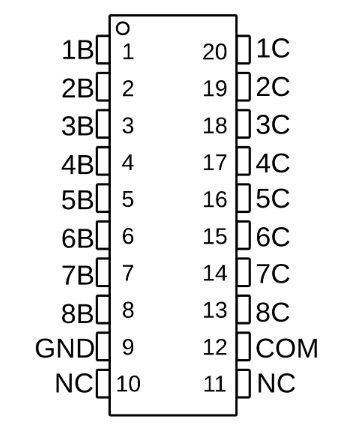
ULN2803CDWR Pin Configuration
Internal Structure and Operation of Each Channel
To understand how the device operates internally, we will explore the schematic for one of the eight identical channels.
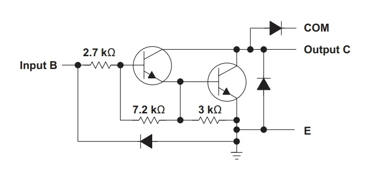
ULN2803CDWR Functional Block Diagram
At the core of each channel is a Darlington pair composed of two NPN transistors. The emitter of the first (pre-driver) transistor connects to the base of the second (main output) transistor. This configuration provides a very high current gain, allowing a small input current (in the microamp range) to control a significantly larger output current. The input stage incorporates a network of three resistors:
- 2.7 kΩ resistor: Acts as a series base resistor, limiting the input current when driven by a logic signal (e.g., from a 5 V MCU GPIO pin).
- 7.2 kΩ and 3 kΩ resistors: Function as base-emitter pulldown resistors. They divert small leakage currents to ground, ensuring the Darlington pair remains fully off when the input signal is low or floating—this prevents unintended activation of the output.
Each output pin features an integrated freewheeling (flyback) diode connected to the common COM pin. When switching inductive loads, the collapsing magnetic field generates voltage spikes that are clamped by this diode, safely directing the energy to the supply and protecting the output transistor.
Additionally, the device contains internal protection diodes between the base-emitter and collector-emitter junctions. These are normally reverse-biased, but if forward-biased by excessive voltages, parasitic NPN transistors may conduct, drawing current from other pins and causing unintended cross-conduction. Maintaining signals within recommended voltage limits ensures proper isolation and reliable operation.
ULN2803CDWR: Maximum Ratings and Operating Characteristics
The maximum ratings define the limits within which the transistor can function without risking permanent damage or failure. Exposure to absolute maximum-rated conditions for extended periods may affect device reliability. Here are the functional and thermal ratings from the datasheet.
When designing with ULN2803ADWR or the ULN2803CDWR replacement, referencing the original datasheet ensures correct footprint, pinout, and 3D model alignment.
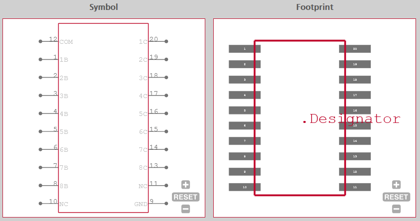
ULN2803CDWR schematic symbol and footprint from UL
If you’re looking for more information on the ULN2803ADWR replacement or the ULN2803CDWR datasheet, Ultra Librarian helps by compiling all your sourcing and CAD information in one place. Our platform provides verified, ready-to-use footprints, symbols, and 3D models that support all popular ECAD applications, along with sourcing information from worldwide distributors.
Working with Ultra Librarian sets your team up for success, ensuring streamlined and error-free design, production, and sourcing. Register today for free.


")
")