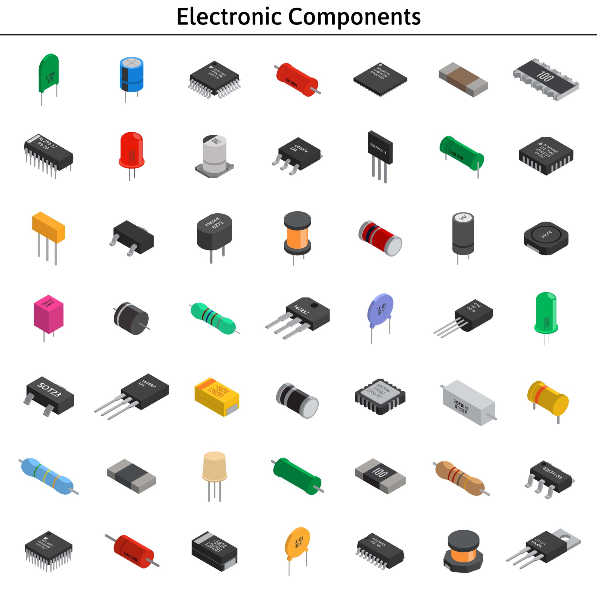
When designing printed circuit boards, physical package dimensions directly dictate component density, thermal dissipation, and manufacturing yield. Utilizing a standardized SMT Components Size Chart helps hardware engineers select surface-mount devices (SMDs) that balance circuit performance with real-world fabrication limits.
Surface-mount technology (SMT) relies heavily on passive components (e.g., resistors, capacitors, and inductors). However, industry confusion frequently arises because both imperial and metric naming systems use four-digit identifiers for different physical dimensions. Understanding these package codes, along with Design for Manufacturability (DFM) rules, helps prevent costly assembly failures such as tombstoning, solder bridging, or component misplacement.
Standard SMT Components Size Chart
The table below details standard two-terminal discrete SMT packages (resistors, capacitors, and inductors). It maps imperial package codes to their metric equivalents and provides physical dimensions alongside industry application categories.
| SMD Package (Imperial) | Metric Equivalent | Dimensions (mm) | Dimensions (in) | Industry Application & Commonality |
| 01005 | 0402 Metric | 0.4 x 0.2 | 0.016 x 0.008 | Ultra-Miniature / Niche (Smartphones, wearable RF modules) |
| 015015 | 0404 Metric | 0.4 x 0.4 | 0.015 x 0.015 | Ultra-Miniature / Specialized RF decoupling |
| 0201 | 0603 Metric | 0.6 x 0.3 | 0.024 x 0.012 | High-Density Mobile / Advanced consumer electronics |
| 0202 | 0505 Metric | 0.5 x 0.5 | 0.020 x 0.020 | Specialized High-Frequency RF passives |
| 02404 | 0610 Metric | 0.6 x 1.0 | 0.024 x 0.039 | Specialized Wide-Termination passives |
| 0303 | 0808 Metric | 0.8 x 0.8 | 0.031 x 0.031 | Specialized Compact Array passives |
| 0402 | 1005 Metric | 1.0 x 0.5 | 0.039 x 0.020 | Standard SMT (Most common for high-density PCBs) |
| 0603 | 1608 Metric | 1.6 x 0.8 | 0.063 x 0.031 | Standard SMT (Industry standard for general electronics) |
| 0805 | 2012 Metric | 2.0 x 1.25 | 0.079 x 0.049 | Standard SMT (Prototyping, power indicators, higher power) |
| 1008 | 2520 Metric | 2.5 x 2.0 | 0.098 x 0.079 | Medium Power / Inductors and filtering networks |
| 1111 | 2828 Metric | 2.8 x 2.8 | 0.110 x 0.110 | High-Q RF Capacitors / Specialized microwave circuits |
| 1206 | 3216 Metric | 3.2 x 1.6 | 0.126 x 0.063 | Standard SMT (Power rails, current sensing, 0.25W resistors) |
| 1210 | 3225 Metric | 3.2 x 2.5 | 0.126 x 0.098 | High Power / Surge suppression, bulk decoupling |
| 1806 | 4516 Metric | 4.5 x 1.6 | 0.177 x 0.063 | High Power / Specialized filter networks |
| 1808 | 4520 Metric | 4.5 x 2.0 | 0.177 x 0.079 | High Voltage / Safety-rated ceramic capacitors |
| 1812 | 4532 Metric | 4.5 x 3.2 | 0.177 x 0.126 | High Power / Transient voltage suppression (TVS) |
| 1825 | 4564 Metric | 4.5 x 6.4 | 0.177 x 0.252 | High Power / Heavy filtering and power distribution |
| 2010 | 5025 Metric | 5.0 x 2.5 | 0.197 x 0.098 | High Power / 0.75W power sense resistors |
| 2512 | 6332 Metric | 6.3 x 3.2 | 0.248 x 0.126 | High Power / 1.0W+ low-CR current sense resistors |
| 2725 | 6963 Metric | 6.9 x 6.3 | 0.272 x 0.248 | Ultra-High Power / Industrial current shunts |
| 2920 | 7451 Metric | 7.4 x 5.1 | 0.291 x 0.201 | High Power / Specialized resettable fuses (PTCs) |
(Note: Always confirm whether a datasheet references Imperial or Metric codes. For example, an “0402 Metric” component is significantly smaller than an “0402 Imperial” component.)
Package Classification Breakdown
1. Ultra-Miniature / Niche Packages (01005 to 0201)
Components in this tier are deployed primarily in ultra-dense mobile devices, hearing aids, and high-frequency RF modules. While these packages minimize board real estate, they dramatically increase manufacturing complexity. Assembly requires high-precision optical pick-and-place machines, ultra-fine solder paste (Type 4 or Type 5), and specialized inspection equipment.
2. Standard Mainstream SMT Packages (0402 to 1206)
These packages represent the vast majority of surface-mount passives used in commercial, industrial, and automotive electronics.
- 0402: Preferred for dense consumer products where space is limited.
- 0603: The most widely used general-purpose package, balancing small footprint size with easy hand-rework capability.
- 0805 & 1206: Selected for power distribution lines, LED indicators, or circuits requiring higher power ratings (0.125W to 0.25W).
3. High-Power and Current-Sensing Packages (1210 to 2512)
Larger discrete packages provide higher thermal dissipation and wider physical terminal spacing. Packages like 2010 and 2512 are chosen specifically for low-milliohm current-sensing resistors, high-voltage ceramic capacitors, and power supply snubber circuits where thermal management is essential.
How Component Size Impacts PCB Development
Component selection influences every stage of the printed circuit board assembly (PCBA) lifecycle: Design, Build, and Test (DBT). In many PCB designs, choosing between surface-mount and through-hole components comes down to size. Surface-mount devices (SMDs) are generally smaller, allowing higher component density and more compact products.
1. PCB Manufacturing Considerations (DFM)
From a manufacturing perspective, surface-mount components enable highly automated assembly. Bulk reel packaging and pick-and-place machines minimize manual handling while reducing soldering errors during SMT assembly.
- Thermal Mass and Tombstoning: Tombstoning occurs during reflow soldering when a small component (such as a 0402 or 0201) lifts vertically on one end. Such a defect is caused by uneven surface tension in molten solder (e.g., when one pad connects directly to a large ground plane while the other connects to a thin trace). Designers must use thermal relief connections in copper pours to ensure equal thermal mass across both pads.
- IPC-7351 Courtyard Boundaries: IPC-7351 guidelines define an excess clearance area (courtyard) around each footprint pad. Placing 0805 or 1206 components too close together prevents proper fillet formation and impedes visual inspection.
- Component Clearances: Minimum clearance between passive components typically ranges from 0.25 mm for 0402 packages up to 0.50 mm or more for 1206 and larger packages.
2. PCB Assembly Considerations (DFA)
Smaller components increase board density, but require tighter manufacturing tolerances across processes ranging from pick-and-place accuracy to solder paste deposition and reflow profiling.
- Pick-and-Place Machine Capabilities: Automated SMT placement equipment utilizes vacuum nozzles to transport parts from tape reels to the PCB. Placing 01005 or 0201 packages requires specialized micro-nozzles and high-resolution vision systems.
- Solder Paste Stencil Thickness: Stencil foil thickness (typically 4-6 mils) dictates solder paste volume. Mixing ultra-small 0201 packages with large power ICs on the same board creates a stencil aperture conflict: a 6-mil stencil deposits too much paste on 0201 pads (causing short circuits), whereas a 4-mil stencil deposits insufficient paste on large IC leads.
- Solder Bridging vs. Cold Joints: Reflow temperature profiles must be tuned to the component mix. Larger packages require more heat to reach the liquidus temperature than small passives.
3. PCB Testing Considerations (DFT)
Testing is the final step before a PCB enters production. While test engineers typically perform post-manufacturing testing, inspections also occur throughout fabrication and assembly. For SMT components, testing, especially functional testing, can be more challenging due to their small size and high component density.
- In-Circuit Test (ICT) Access: Automated bed-of-nails and flying-probe testers require physical access to the test points. Testing signals directly on small component pads (such as 0402 or 0201) risks damaging the component or giving false open-circuit readings.
- Test Point Clearance: Designers must route net signals to dedicated test pads (minimum diameter 0.7 mm to 1.0 mm) spaced at least 1.27 mm apart, keeping test points clear of high-profile components.
- Automated Optical Inspection (AOI): Smaller component packages increase reliance on high-resolution AOI and Automated X-ray Inspection (AXI) machines to verify solder joint integrity and component alignment.
Standard IC Packages and IPC-7351 Compliance
While the SMT Components Size Chart covers discrete two-terminal parts, integrated circuit (IC) packaging also follows strict standardization:
- Small Outline Packages (SOIC, SSOP, TSSOP): Gull-wing leaded packages with pin pitches ranging from 1.27 mm down to 0.65 mm.
- No-Lead Packages (QFN, DFN): Flat plastic packages with bottom-exposed pads that maximize thermal transfer and minimize board area.
- Ball Grid Arrays (BGA): High-density packages utilizing an array of solder balls beneath the IC body.
Integrating multi-component ICs or resistor networks reduces total component count, simplifying layout routing while saving valuable board real estate. Adhering to IPC-7351 footprint standards guarantees that land patterns accommodate manufacturing tolerances for all IC and discrete package types.
Best Practices for Selecting SMT Component Sizes
Selecting the right SMT package size requires balancing electrical, mechanical, and manufacturing requirements. Following a few proven design practices helps improve assembly yield, simplify sourcing, and reduce the risk of costly PCB revisions.
- Standardize on 0603 or 0402 for General Passives: Utilize 0603 components for general prototyping and lower-volume production; select 0402 for space-constrained production designs.
- Avoid 0201 and 01005 Unless Necessary: Reserve ultra-miniature packages for designs where board area is at an absolute premium.
- Check CM Equipment Capabilities Early: Confirm your Contract Manufacturer’s minimum component size, stencil thickness options, and placement tolerances before finalizing the layout.
- Match Package Size to Power Requirements: Verify resistor power ratings (e.g., 1/16W for 0402, 1/10W for 0603, 1/8W for 0805, 1/4W for 1206) and capacitor voltage ratings before layout.
- Utilize Verified Footprint Libraries: Download pre-validated CAD footprints that comply with IPC-7351 standards to prevent pad-mismatch errors.
Find Verified SMT CAD Models and Footprints
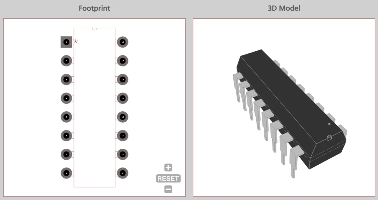
After selecting component package dimensions using the SMT Components Size Chart, ensure your design incorporates verified land patterns and 3D STEP models. Working with Ultra Librarian provides instant access to pre-cleared schematic symbols, footprints, and 3D models compatible with all major ECAD tools. You can also verify distributor stock levels and pricing directly through Ultra Librarian, so register today for free.
Working with Ultra Librarian sets your team up for success, ensuring streamlined and error-free design, production, and sourcing. Register today for free.

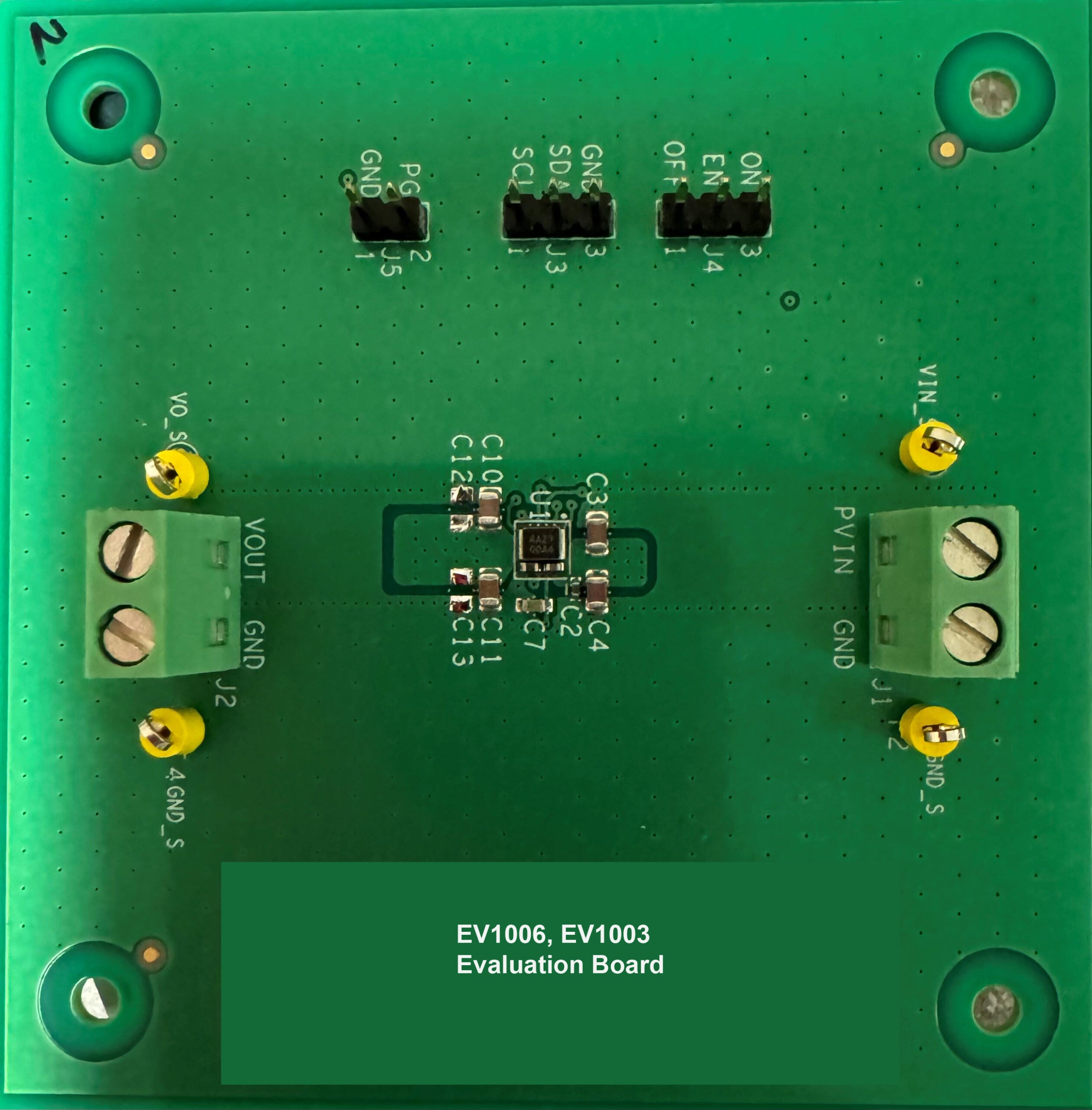
 If you’re looking for any of our component footprints or models, we have readily available and free options for you and your design team. Search our library for the solution you’ve been looking for.