
Building hardware for motor drives, consumer gadgets, or factory controls takes a reliable computing core. You might already be familiar with the STM32F103C8T6 chip from the popular, low-cost prototyping board known as the “Blue Pill.” But using the STM32F103C8T6 when designing your own custom printed circuit board (PCB) is a whole new ballgame. Once you lay out your own copper traces, it’s vital that you thoroughly understand the STM32F103C8T6 datasheet.
Ignore decoupling guidelines or shortcut the crystal layout, and you will see it on the bench: erratic resets, failed USB enumerations, and degraded analog-to-digital converter (ADC) readings. The datasheet tells you exactly how to avoid these failures. This article walks through the sections that matter most.
STM32F103C8T6 Datasheet Core Specifications
| Parameter | Value |
| Core | 32-bit ARM Cortex-M3 |
| Max Clock | 72 MHz |
| Flash / SRAM | 64 KB / 20 KB |
| Supply Voltage | 2.0 V to 3.6 V |
| Package | LQFP48, 7×7 mm, 0.5 mm pitch |
| ADC | Two 12-bit converters, up to 10 channels |
| Interfaces | USB, CAN, 2x SPI, 2x I2C, 3x USART |
| Temp Range (standard) | -40°C to +85°C |
| Temp Range (extended) | -40°C to +105°C |
The STM32F103C8T6 offers two 12-bit ADCs, three general-purpose 16-bit timers plus one PWM timer, and standard communication interfaces including I2C, SPI, USART, USB, and CAN.
Power Supply Design and Noise Suppression
The STM32F103C8T6 operates from a 2.0-3.6 V power supply. The datasheet notes strict separation between the primary digital supply domain (VDD) and the analog supply domain (VDDA). Mixing high-frequency digital switching noise into the analog rail directly degrades the performance of the internal 12-bit ADCs. On a busy board, this is the difference between a clean 12-bit conversion and one that looks like it was measured through a wall socket.
High-Frequency Decoupling and Trace Geometry
Effective noise suppression comes down to disciplined capacitor placement. You cannot simply drop capacitors near the Microcontroller Unit (MCU) and expect stable operation. The trace length between the capacitor pad, the MCU pin, and the ground return path introduces parasitic inductance, destroying the high-frequency filtering capability. To avoid this, follow these decoupling guidelines for the STM32F103C8T6:
- Digital Supply (VDD): Place one 100 nF ceramic capacitor directly adjacent to every VDD pin. Keep these components on the same PCB layer as the MCU to avoid via inductance.
- Bulk Capacitance: Position at least one 10 µF bulk capacitor near the low-dropout (LDO) regulator feeding the MCU to handle larger transient current spikes.
- Analog Supply (VDDA): Route the analog power through a separate trace. Place a 1 µF capacitor in parallel with a 10 nF capacitor between VDDA and VSSA.
- Noisy Environments: Add a ferrite bead in series with the VDDA trace when the board includes switching regulators or other high-frequency noise sources.
Crystal Oscillator Layout and Clock Circuitry
Both the 8 MHz High-Speed External (HSE) and the 32.768 kHz Low-Speed External (LSE) oscillators are susceptible to interference. Misrouted signals near these crystals act as an antenna, coupling noise directly into the oscillation loop and potentially causing clock jitter or startup failure. To prevent this, you should surround the oscillator circuitry with a ground guard ring and ensure no high-speed digital traces run on the copper layers directly beneath the crystal components.
While the STM32F103C8T6 datasheet defines the electrical limits for the internal oscillator driver, it cannot provide the specific load capacitance (CL) for your chosen crystal. You must pull that value from the crystal manufacturer’s documentation (e.g., an Abracon or Epson datasheet) to accurately calculate your external capacitor values.While the STM32F103C8T6 datasheet defines the electrical limits for the internal oscillator driver, it cannot provide the specific load capacitance (CL) for your chosen crystal. You must pull that value from the crystal manufacturer’s documentation (e.g., an Abracon or Epson datasheet) to accurately calculate your external capacitor values.
To keep your timing signal clean, follow these layout requirements:
- Keep traces for both the HSE and LSE clocks symmetrical and as short as possible to reduce parasitic effects.
- Place the crystal and its load capacitors on the same side of the PCB as the microcontroller to avoid using vias, which add unnecessary inductance.
- Calculate your external capacitor values by accounting for board-level stray capacitance, which typically adds 2 pF to 7 pF to the loop.
- Avoid placing the crystals near the edges of the board or near high-current switching paths to minimize electromagnetic interference (EMI).
- Consult proven reference designs for the LQFP48 package to see how others have successfully isolated these sensitive analog nodes.
Essential Clock Parameters
| Feature | Component / Specification | Typical Load Capacitance | Layout Requirement |
| HSE Clock | 8 MHz Crystal | ~20 pF (per crystal spec) | Symmetrical trace lengths, GND guard ring |
| LSE Clock | 32.768 kHz Crystal | ~7-12.5 pF (per crystal spec) | Placed close to PC14/PC15; no underlying signal traces |
| NRST Pin | 10 kΩ pull-up to VDD, 100 nF to GND | N/A | Capacitor placed close to pin to prevent false resets |
Hardware Boot Configuration and Reset Logic
When setting up the STM32F103C8T6 for a specific boot configuration, you must define the hardware state of two dedicated pins during the reset sequence. The internal logic samples the BOOT0 and BOOT1 pins on the fourth rising edge of the system clock after a reset. This hardware-level check tells the microcontroller whether to start from the main Flash memory, the system memory (built-in bootloader), or the internal SRAM.
For standard operation, pull BOOT0 to ground through a 10 kΩ resistor. For field firmware updates via UART, design in a jumper or a small pushbutton that pulls BOOT0 to VDD while keeping BOOT1 (pin PB2) tied to ground. While the STM32F103C8T6 Datasheet lists SRAM boot as an option by pulling both pins high, most developers stick to Flash or the system bootloader for stability. Always include a 100 nF capacitor on the NRST pin to prevent stray noise from triggering an unexpected reboot.
GPIO Pin Assignments and Peripheral Routing
The STM32F103C8T6 provides 37 fast I/O ports, serial wire debug (SWD) and JTAG interfaces, two SPI interfaces, two I2C interfaces, three USART interfaces, one USB interface, and one CAN interface. With that many peripherals sharing a 48-pin package, pin assignment strategy matters before you touch the PCB layout. Lock down your high-speed interfaces and debug headers first. Assigning those pins after physical PCB routing forces awkward routing compromises.
The Serial Wire Debug (SWD) interface is mandatory for programming and debugging the Cortex-M3 core. SWD requires two pins: SWDIO on PA13 and SWCLK on PA14. Route both to a standard debug header — a 10-pin Cortex or a simple 4-pin header both work. Proper planning here aligns with smart component decision-making from the onset of schematic capture.
For the higher-speed interfaces, apply these routing rules:
- USB 2.0 Full-Speed (PA11/PA12): Route D- and D+ as a differential pair. The trace impedance should be matched to the USB cable differential impedance, which is nominally 90 ohms for the signal pair.
- Note that the STM32F103C8T6 has an internal USB physical layer (PHY) with embedded output impedance matching. Matching output impedance is already embedded in the pad transceiver and is in line with the USB specification; no external resistors are needed.
- Length Matching: Ensure D+ and D- traces are equal length to prevent skew. Length mismatches should be kept under 0.5 mm for USB 2.0.
- Via Reduction: Minimize vias on the differential pair. Each via introduces an impedance discontinuity that reflects signal energy back toward the source.
- CAN Bus: The STM32F103C8T6 includes a CAN controller but requires an external transceiver integrated circuit (IC) for the physical layer. Route CAN TX and CAN RX cleanly to the transceiver and keep the CAN TX and CAN RX traces away from analog inputs. Cross-referencing IC manufacturer codes can help identify and source the correct transceiver variants for your application.
STM32F103C8T6 Datasheet Thermal Ratings and LQFP48 Footprint
The STM32F103C8T6 is available in both the -40 to +85°C temperature range and the -40 to +105°C extended temperature range. For industrial deployments, verify the specific part suffix you are ordering — the standard “C8T6” suffix covers the -40 to +85°C range. The extended temperature variant uses a different order code.
The Cortex-M3 is efficient, but running at 72 MHz while driving multiple general-purpose input/output (GPIO) pins under load does generate localized heat. Therefore, use a continuous ground plane as a practical heatsink. Connect all VSS pins directly to a solid internal ground plane using multiple vias to keep thermal resistance low and provide a clean return path for switching currents simultaneously.
LQFP48 Footprint Checklist
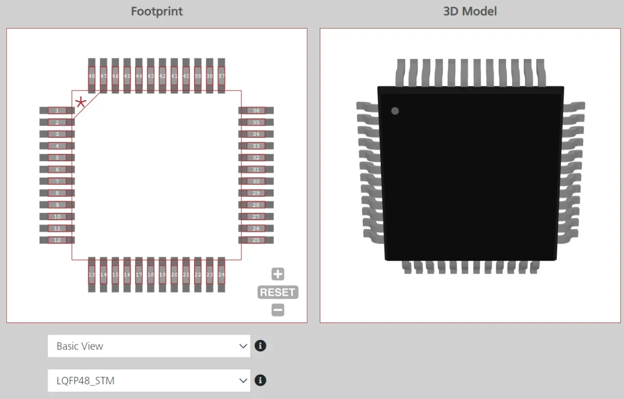
The maximum power dissipation of the STM32F103C8T6 is 363 mW. The 0.5 mm pin pitch leaves very little room for error. A pad that is even slightly too wide causes solder bridges, and a pad that is too narrow produces a cold joint under reflow. Follow this checklist to get your pads right and to ensure you efficiently dissipate power from the LQFP48 chip.
- Verify pad dimensions against the mechanical drawings in the official STMicroelectronics datasheet.
- Confirm the solder paste mask provides adequate aperture coverage without overlap between adjacent pads.
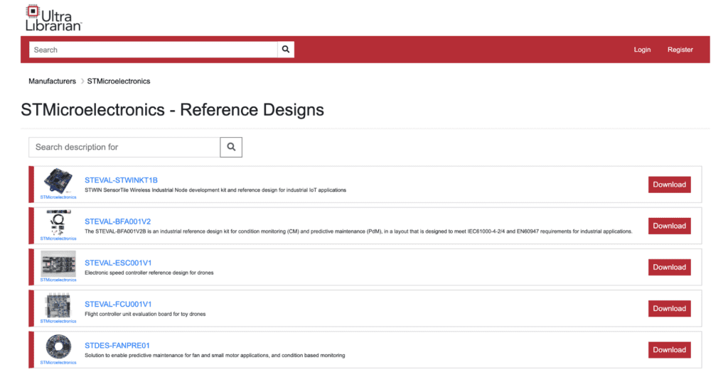
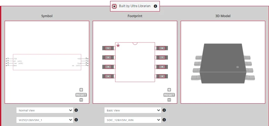
- Use a verified, manufacturer-approved LQFP48 footprint. You can download a certified model directly from the STM32F103C8T6 page on Ultra Librarian.
- Run a design rule check (DRC) to confirm all clearance tolerances are met before generating fabrication outputs. If building out your surrounding modules, consult reference designs to ensure compliant footprints across your entire BOM.
From Datasheet to Production-Ready Board
Strict adherence to the layout constraints defined in the STM32F103C8T6 datasheet ensures your custom hardware maintains stable signal integrity and reliable peripheral performance in the first revision.
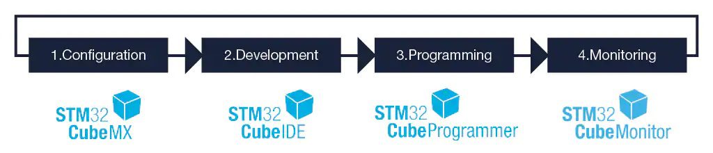
Before locking the layout, cross-reference your pin assignments against STM32CubeMX. The tool validates peripheral pin compatibility against the actual silicon and flags conflicts before they become a costly board respin. Combine that with a verified CAD footprint and the guidelines in this article, and your first custom STM32 board has a strong foundation to succeed on the first pass.
Moving from a schematic to a production-ready board requires more than just reading the STM32F103C8T6 datasheet — it requires accurate models to support your design choices. Ready to secure your layout? Download verified footprints and 3D models compatible with all popular ECAD applications, and seamlessly transition to procurement through our worldwide distributors. Start your design with confidence at Ultra Librarian.
Working with Ultra Librarian sets your team up for success, ensuring streamlined and error-free design, production, and sourcing. Register today for free.

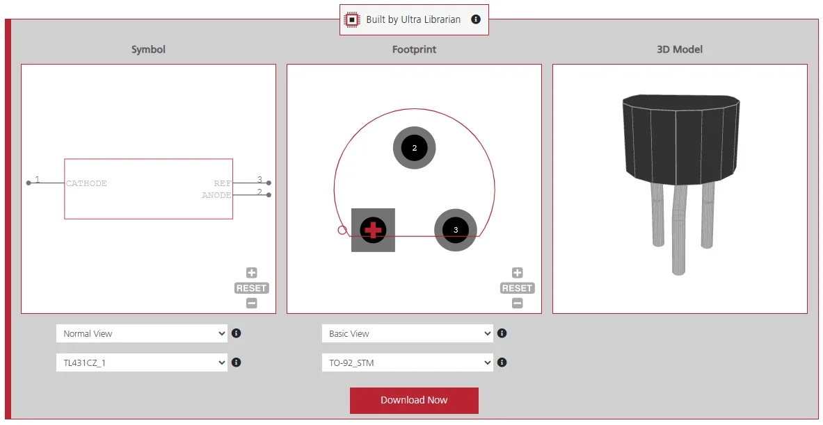
 If you’re looking for any of our component footprints or models, we have readily available and free options for you and your design team. Search our library for the solution you’ve been looking for.