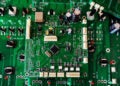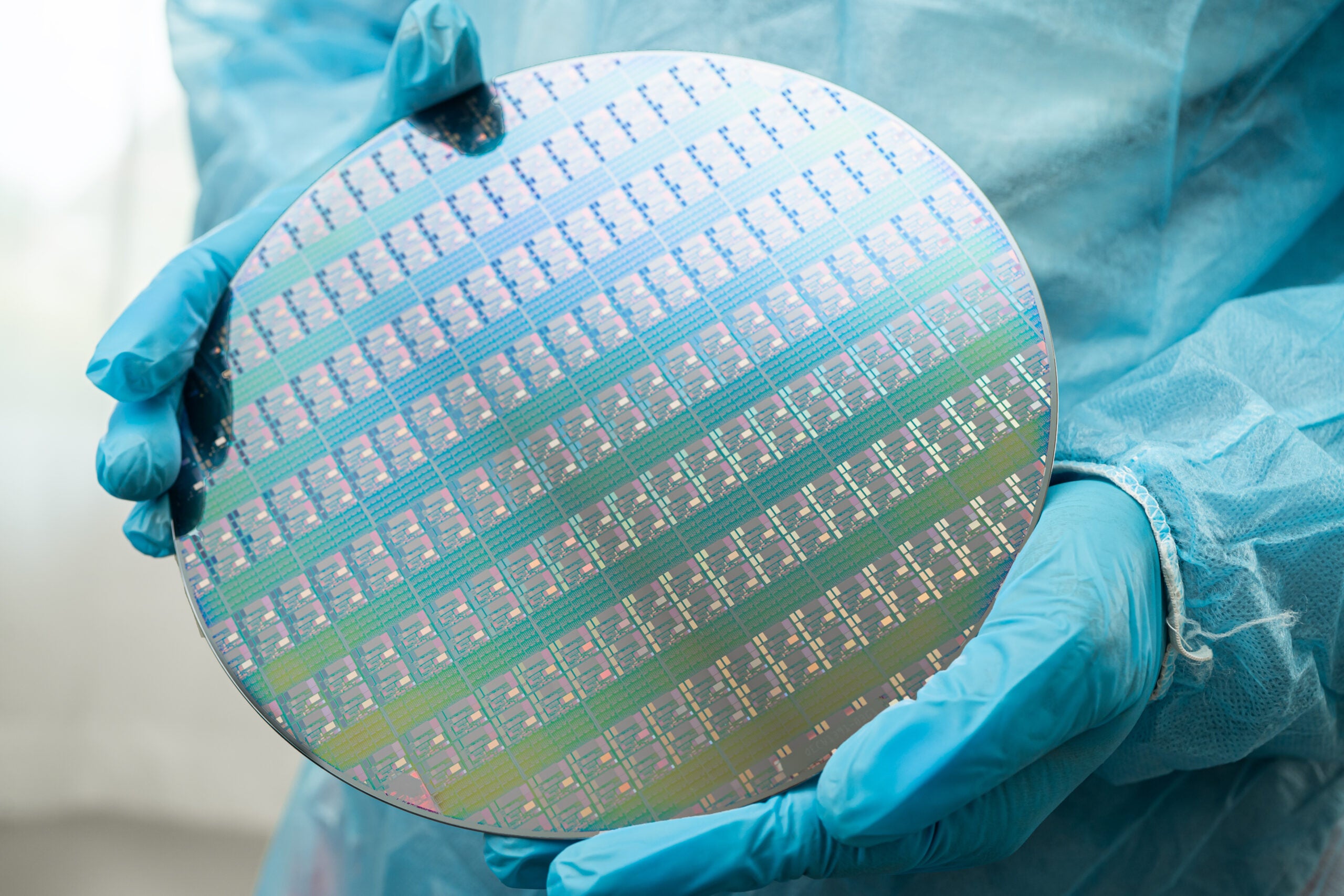
Electronic component semiconductor silicon wafer
It is indisputable that the invention of the transistor opened the door for the current technological revolution. Today, it is becoming increasingly difficult to find products that do not leverage electronics to enhance capabilities and functionality. More often than not, these products and systems are driven by circuit boards that include transistors or other semiconductors. The importance of semiconductors is evidenced by the success and growth of their manufacturers. These companies transform silicon, germanium, gallium-arsenide, and other semiconductor materials into the most commonly used PCB semiconductors: diodes, transistors, and integrated circuits. By understanding their key attributes and following good design guidelines, you can best utilize electronic components semiconductors in your circuit board and/or product design.Common Electronic Component Semiconductors
Semiconductive materials fall somewhere between insulators, which are highly resistive to current flow, and conductors, which are minimally resistant. Other than passive parts that only dissipate power, like resistors and capacitors, discrete and active semiconductors are the most commonly used components in electronic circuits. Here are the attributes of the most common electronic component semiconductors:| Electronic Components Semiconductor Attributes | |||
| Attributes | Diode | Transistor | Integrated Circuit (IC) |
| Common Types |
|
|
|
| Typical Applications | Rectifiers, Voltage regulators, Demodulators, Switches | Amplifiers, Switches | Microprocessors (MPUs), Control circuitry, signal processing, component arrays, complex circuits |
| Examples | |||
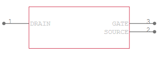
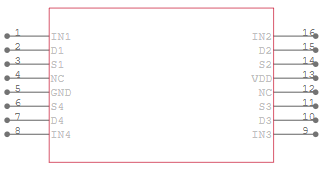
| Component | 1N5230B Zener Diode | 2N5459 JFET Transistor | ADG811YRUZ Analog IC |
| Schematic Symbol |  |
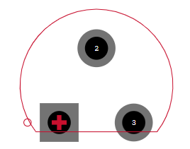
 |
 |
| PCB Footprint | 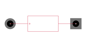 |
 |
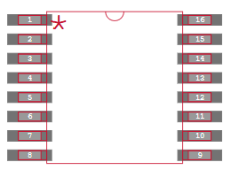 |
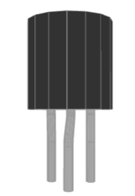
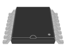
| 3D Model* | 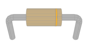 |
 |
 |